Powering today’s microprocessors: Old myths versus modern technology
phase converters running at 1 MHz per phase, using 2-mΩ MOSFETS and 100-nH SMT inductors to deliver 150A at 1V are no longer a novelty. However, they are relatively inefficient and cannot be packed tightly on the PCB due to excessive heating. Thus, the higher switching frequencies that allow smaller inductors and decoupling capacitors do not necessarily translate into a reduction in board space. And even though the output ripple requirements can be met with fewer capacitors, the transient response constraints are now more severe, requiring an increase in costly decoupling capacitors. So despite these technology advances, CPU power design challenges are still there. Fortunately, smart modern technology has also resulted in dual edge pulse-width modulation (PWM) controllers that can be the answer to these challenges.
But before getting any further into the dual-edge modulation solution, let’s have a quick look at the standard trailing-edge modulation scheme and understand why a higher switching frequency is desirable for fast transient response. The leading edge modulation, being somewhat similar to the trailing edge, will not be discussed.
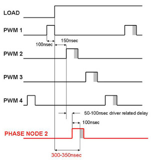
To keep things simple, a 4-phase buck converter switching at 1 MHz is considered. 12V input and 1.2V output is assumed and, neglecting losses, this accounts for 10% duty cycle or 100-nsec on-time. This situation is depicted in
signals labeled PWM1 to PWM4 are the PWM signals the controller sends to the MOSFET drivers. Suppose now that a load step increase occurs right at the moment when PWM1 signal goes down. With the above assumptions, in this conventional trailing edge topology the next PWM signal will appear on the adjacent phase after 150 nsec. The corresponding phase node will go high 50 to 100 nsec later due to the delay introduced by the MOSFET driver and MOSFET. Add to this delay another 100 nsec due to the duty cycle prior to the load increase and now it is clear that the phase will start to react to the load increase 300 to 350 nsec after its occurrence.
During this time the output capacitors will have to be able to supply the extra current and only after this delay will the converter start to increase its duty cycle as a response to the load step. This delay would be significantly longer for a 300-kHz switching frequency. Doubling the switching frequency to 2 MHz helps reduce this delay, but will not cut it in half. Due to the driver related delay, it will become 175 to 225 nsec. This is a very good number and 2-MHz switching frequency is quite achievable with components available today
What else gets better at higher switching frequency? A lower inductance can be used without sacrificing ripple. This allows for a higher dI/dt thus having a direct and positive impact on transient response.
Size is the other aspect that matters and 2-MHz switching frequency allows for smaller inductors and also reduced decoupling.
All these seem to convey the message that 2-MHz, or even higher, is the way to go. Not so when efficiency is taken into account. Even with the super-fast components available today, switching losses now become an important part of the whole picture, with all the above benefits fading away when the converter needs to dissipate 50W instead of 30W.
Therefore, before choosing the power solution for a CPU, the user should be aware of the pros and cons associated with such an approach and also investigate an alternate solution that is now possible based on dual edge modulation.
The dual-edge PWM is probably the most important breakthrough since the adoption of the droop (load line or adaptive voltage positioning (AVP)) concept. It combines the advantages of both trailing edge and leading edge methods without having the disadvantage of using a fixed clock. For steady loads, the clock governs the sequence and timing of all phases and the waveforms look exactly as the ones belonging to a trailing edge or leading edge system. What makes the dual edge system quite different is its behavior during a transient load
event. When a load step occurs, depending on the magnitude, one or even all phases can be turned on simultaneously.
an
d
d
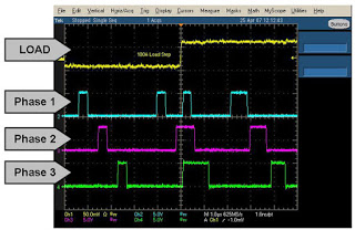
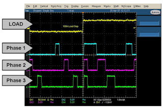
show the response of a 4-phase controller to a 100A step. (The four channel scope allowed the load current and only three phases to be shown.) The converter used in this example switches at 300 kHz per phase. The event captured in
shows the load step occurring soon after phase 2 has been turned on. The controller detects the transient and maintains phase 2 turned on, but also turns on the other phases to help supply the extra current required by the load. The scope shot in
captured another moment when the load transient hit in between and no phase happened to be on at that moment. The controller reacts again and turns all phases on.
The number of phases that can be turned on simultaneously and the conduction time of each phase depend on load step amplitude, slew rate and the moment of occurrence.
The long delay that was present in the previously mentioned conventional trailing edge approach is now basically reduced to the delay introduced by the MOSFETs and their drivers. The response is not only faster (less than 150 nsec total), but by having more phases turned on in the same time, additional faster current can be supplied to the load. Because the effective inductance is reduced by a factor equal to the number of phases that are simultaneously turned on, this converter can achieve a high dI/dt without making use of low value inductors like the ones using conventional modulation techniques. The immediate benefit deriving from this is a more relaxed requirement for the output capacitors. The transient specs for a step of 100A can be met even without using any bulk capacitors if board layout is carefully designed. Good ceramic capacitors are enough to supply the required current during the initial portion of the load step.
After the transient event, the controller comes back to its steady state mode and phases are alternately turned on, although with a higher duty cycle in order to supply the higher current. The absence of any latches enables the controller to shift smoothly between “steady state” and “all phases-on” modes as required by the magnitude and steepness of the load step.
Due to this remarkable ability to respond to transients, converters using the dual edge modulation do not need to use a high switching frequency. Switching frequencies in the 250 to 400 kHz range are quite adequate for most CPU applications. This means savings for the motherboard vendor because efficiency can still be high even without using “best in class” MOSFETs.
When dealing with load transients, there is another aspect that deserves some consideration – the transition from a high to a low current level. This is commonly called the load release. The role of the controller during such an event is basically nonexistent. All it can do is turn on all the low side MOSFETs and wait until the high current, that was flowing through the output inductors prior to the load release, decreases to the low level now required by the load. The current surplus cannot simply disappear and must go somewhere. The only path available is to flow into the output capacitors charging them. This will create an overshoot and in order to keep its magnitude within limits, a certain amount of bulk capacitance is required. This process depends on the value of the output inductors and of course the output voltage level. Since this is a basic energy transfer from the inductors to the output capacitors, it implies that lower value inductors and higher output capacitance will help minimize the overshoot. It is interesting to note that when using the dual edge modulation technique, meeting the droop requirements calls for less output capacitance than what is needed to contain the overshoot.
The overshoot during the load release occurs in the same way even when using standard modulation schemes, but given the larger amount of capacitance used by those systems to meet the droop specs, the overshoot is usually a minor problem.
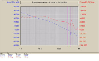
Of course the question is: what can the user do when using a dual edge modulation solution in order to maintain a minimal decoupling without exceeding the overshoot specs? As already mentioned, decreasing the inductance value will help and depending on other factors may also bring additional benefits. A lower inductance directly implies the output ripple will increase, therefore a switching frequency increase is necessary to compensate, but there is no need to go excessively high because super-low ESR (equivalent series resistance) ceramic capacitors now available. Using 220-nH inductors and switching at around 400 kHz can keep the ripple under the 10 mV benchmark while also keeping decoupling to a minimum. Low inductance and light decoupling allow for a very fast compensation loop.
shows what can be expected in terms of loop performance from such a converter: 260 kHz cross-over and 55 degree phase margin while switching at 400 kHz is a hard to achieve set of numbers. For those rare applications where meeting cost is not the main goal, fewer and fewer fortunate engineers face limits when designing a system using dual edge modulation to achieve a 310 kHz cross-over and over 60 degree phase margin while switching at just 430 kHz. The task of debating the validity or significance of these numbers is left to the purists.
However, most of the time, today’s competition rules dictate that the winner is not the highest performance system, but one that meets adequate performance with minimal cost. Usually efficiency, transient response and size are the constraints. In order to comply while keeping cost down, a compromise is often needed. Maybe a couple more bulk or ceramic capacitors are required, or maybe
a change in switching frequency or inductance value is needed. A good layout can help a lot too. These are variables that can be played with even when using the standard trailing or leading edge modulation, but they can lead to a much more cost effective solution when also taking advantage of the capabilities the dual edge modulation can bring in.
a change in switching frequency or inductance value is needed. A good layout can help a lot too. These are variables that can be played with even when using the standard trailing or leading edge modulation, but they can lead to a much more cost effective solution when also taking advantage of the capabilities the dual edge modulation can bring in.
Dual edge PWM controllers can offer unprecedented performance in terms of transient response for lower cost while succeeding in enabling lower switching frequencies for improved efficiency. Controllers using true dual edge or somewhat different, but basically equivalent modulation, are in production today and find their well-deserved seat in more and more applications as users start to become aware of their benefits.


