System-on-Chip
BY
JULIANA GJANCI
B.S. University of Illinois at Chicago, 2006
THESIS
Submitted as partial fulfillment of the requirements
For the degree of Master of Science in Electrical and Computer Engineering
In the Graduate College of the
University of Illinois at Chicago, 2008
Chicago, Illinois
i
© Copyright by JULIANA GJANCI 2008
All Rights Reserved
ii

ABSTRACT
On-Chip Voltage Regulation for Power Management in System-On-Chip
JULIANA GJANCI
The scaling of minimum feature sizes down to nanometer range and the spiraling
frequencies in GHz scale has lead to system-on-a-chip (SOC) implementation for many
emerging applications. To utilize the unprecedented computing power of over billion transistors
on each SOC die many integrated circuit (IC) implementations have been adopting multi-core
strategies instead of single-core implementation. It is predicted that a network-on-chip (NOC)
communication fabric will be used in such multi-core SOCs. In the coming decades, market
competition among different design paradigms and implementation strategies will resolve itself
as their technical and economical costs and benefits are being widely investigated and
documented. However, ITRS and all the recent studies and roadmaps have indicated that in all
future micro- and nano-electronic circuits and systems power distribution, reliability and
management issues are expected to become the most serious bottlenecks. The frequency
increase as well as convergence towards mixed-signal systems has aggravated the difficulties of
supplying clean power to integrated circuits. Power consumption has a critical impact on IC
performance, and therefore, its management is important. Ineffective power management causes
lower chip performance, increases area and makes the design nonfunctional. Therefore, more
than ever, power integrity is vital in the successful design of today’s electronic systems.
iii
With the growing power management concern in high performance microprocessor
designs the requirement for efficient voltage regulation has become a very critical design
challenge. The objectives of this thesis are to investigate the scopes and techniques for on-chip
voltage regulation in SOC design, and to synthesize a methodology for on-chip voltage
regulator module (VRM) implementation. The approach is primarily based on existing voltage
regulator topologies that are used for off-chip voltage regulation. Here on-chip implementation
and performance of these voltage regulators will be investigated. In order to accomplish these
goals, the following specific tasks have been attempted in this research initiative:
• Perform in-depth analysis of all the available regulator topologies that have been
used for off-chip voltage regulation at the printed circuit board (PCB) level.
• Investigate the best topology suitable for on-chip implementation.
• Synthesize an on-chip design strategy that provides better regulator efficiency and
power management, and minimizes design complexity and cost.
• Investigate the performance implications of placing the regulators on chip.
Aggressive power management is necessary since more devices are packed on a single
processor chip operating at high frequencies. Analysis indicates that a DC/DC step-down
voltage regulator module (VRM) is needed to deliver power from the source to the load, to
provide constant voltage to the load, control power fluctuations, and prevent damages to loads
connected to the supply. Traditionally voltage regulators are off-chip devices due to the large
inductive and capacitive filter elements that they employ. They operate at low switching
frequencies, typically lower than 5MHz, and as a result they fail to perform fast voltage
transitions. Furthermore, on-chip implementation of such regulators employing large inductive
iv
and capacitive elements is not practical due to their complexity and high cost. This is especially
a bottleneck when multiple on-chip power domains are needed.
The methodology proposed in this thesis includes a two-stage converter with the first
stage consisting of a switching voltage regulator located off-chip and the second stage
consisting of a tree linear regulator topology located on-chip. This approach proves to be
efficient, simple, and less costly compared to other options that offer total on-chip integration of
switching regulators. The proposed approach combines the advantages of both voltage regulator
topologies – switching and linear, and results in one hybrid design that is suitable for multi-core
SOC implementations.
v
ACKNOWLEDGMENTS
First, I would like to thank God for all that He has endowed upon me and all the
opportunities that He has presented to me in life. I would like to thank my parents for their
encouragement and support and for creating the opportunity for me to study in the United
States. None of my success would have been possible without them.
I would like to express my gratitude and deepest appreciation to my advisor, Dr. Masud
H. Chowdhury, for his advice, help, support, motivating suggestions and encouragement during
my research. His endless energy and enthusiasm in research has motivated all of his students,
including me. I wish him all the best. It was an honor to have Dr. Ashfaq Khokhar and Dr.
Kaijie Wu in my thesis committee. I am grateful for their comments and objective directions to
complete the Masters Thesis work.
Last but not least, I would like to extend my gratitude to all of the people who have
helped and inspired me during my research, my friends and colleagues especially Nima Jahedi,
who volunteered their time and effort to help me.
vi

TABLE OF CONTENTS
CHAPTER PAGE
LIST OF TABLES………………………………………………………………………………………………………..vii
LIST OF FIGURES……………………………………………………………………………………………………….ix
ABBREVATIONS…………………………………………………………………………………………………………xii
1 INTRODUCTION………………………………………………………………………………………………….13
1.1 Brief Overview of Microprocessor Evolution………………………………………………………13
1.2 Microprocessor Power Delivery and Load Characteristics…………………………………….15
1.3 The Role and Operation of a Voltage Regulator…………………………………………………..18
1.4 Off-Chip VR Alernatives…………………………………………………………………………………..20
1.5 Why On-Chip VR…………………………………………………………………………………………….23
1.5.1 Limitations of Off-Chip Voltage Regulator………………………………………………………24
1.5.2 Limitations of Off-Chip Voltage Regulator………………………………………………………25
1.6 Thesis Outline………………………………………………………………………………………………….26
2 VOLTAGE REGULATOR TOPOLOGIES……………………………………………………………27
2.1 Complete Survey of all On-Chip VRM Topologies………………………………………………28
2.1.1 Linear Regulators………………………………………………………………………………………….28
2.1.2 Switching Regulators…………………………………………………………………………………….30
2.2 Other On-Chip-Friendly VR Topologies……………………………………………………………..31
2.2.1 Switched Capacitor Circuits (Charge Pumps)…………………………………………………..31
2.2.2 MEMS Approach (DC/DC Converters with MEMS Inductors)…………………………..32
2.2.3 Inductor Multiplier Technique………………………………………………………………………..32
2.3 Relative Merits/Demerits of Each Option……………………………………………………………33
2.4 On-Chip VRM Issues………………………………………………………………………………………..34
3 ON-CHIP VRM FOR SINGLE AND DUAL CORE SYSTEMS………………………………36
3.1 Single-Core Voltage Regulation…………………………………………………………………………37
3.2 Buck-Type Switching Regulator for On-Chip Implementation………………………………38
3.3 Implementation Challenges……………………………………………………………………………….41
3.4 Hot Swap Controller Solution…………………………………………………………………………….43
4 TWO-STAGE APPROACH FOR VOLTAGE REGULATOR IMPLEMENTATION
IN SOC………………………………………………………………………………………………………………….47
4.1 Hybrid Two-Stage Regulator……………………………………………………………………………..49
4.2 Stage 1: Switching Regulator…………………………………………………………………………….51
4.2.1 Pulse Width Modulation (PWM)…………………………………………………………………….55
4.2.2 Switching Regulator Efficiency………………………………………………………………………55
4.3 Stage-2: Low Dropout Linear Regulator (LDO)…………………………………………………..57
4.3.1 Pass Element………………………………………………………………………………………………..58
4.3.2 Error Amplifier…………………………………………………………………………………………….61
v
4.3.3 Power Supply Ripple Rejection………………………………………………………………………62
4.3.4 Efficiency of Low Dropout Linear Regulator……………………………………………………63
4.4 Simulation Results and Analysis………………………………………………………………………..64
5 FUTURE WORK…………………………………………………………………………………………………..74
5.1 Power Management and Thermal Stability in Multi-Core Chips…………………………….74
5.2 Efficient Power Gating Techniques for Multi-Core Design……………………………………76
6 CONCLUSION……………………………………………………………………………………………………..81
REFERENCES………………………………………………………………………………………………………………83
vi
LIST OF TABLES
Table 1. Switching Regulator Circuit Parameters…………………………………………………………54
Table 2. LDO regulator efficiency……………………………………………………………………………..64
Table 3. LDO regulator efficiency, parallel design………………………………………………………73
vii

LIST OF FIGURES
FIGURE PAGE
Figure 1-1. Exponential increase of transistors per die………………………………………………….13
Figure 1-2. Current and voltage roadmap for present and future microprocessors……………14
Figure 1-3. Voltage regulator providing power to the microprocessor……………………………16
Figure 1-4. Voltage regulator (VR-down) on motherboard……………………………………………16
Figure 1-5. Voltage regulator module, VRM……………………………………………………………….17
Figure 1-6. Voltage regulator operation………………………………………………………………………19
Figure 1-7. Laptop power supply……………………………………………………………………………….21
Figure 1-8. Circuit of a conventional buck converter……………………………………………………22
Figure 1-9. Circuit of a synchronous buck converter……………………………………………………22
Figure 1-10. Circuit of a multi-phase buck converter……………………………………………………23
Figure 1-11. Off-chip voltage regulator module…………………………………………………………..24
Figure 1-12. On-chip voltage regulator module…………………………………………………………..25
Figure 2-1. Power distribution noise in a system on a chip……………………………………………27
Figure 2-2. Linear regulator………………………………………………………………………………………28
Figure 2-3. Switching regulator…………………………………………………………………………………30
Figure 2-4. Switched capacitor regulator…………………………………………………………………….31
Figure 2-5. Switching regulator employing inductor multiplier……………………………………..32
Figure 3-1. Intel dual core processor, from Intel website………………………………………………36
Figure 3-2. Switching Regulator with hysteresis control……………………………………………….39
Figure 3-3. Inductor Current in Switching Converter……………………………………………………40
ix
Figure 3-4. Regulator off-chip a) without controller and b) with controller…………………….43
Figure 3-5. Regulator and controller on-chip………………………………………………………………44
Figure 3-6. Inrush current effects in the supply and load………………………………………………45
Figure 3-7. Inrush current protection………………………………………………………………………….45
Figure 4-1. STA2052, System-on-chip, from Nikkei Electronics Asia……………………………47
Figure 4-2. Two-stage conversion……………………………………………………………………………..49
Figure 4-3. Switching regulator…………………………………………………………………………………51
Figure 4-4. Switching regulator with switch ON………………………………………………………….52
Figure 4-5. Switching regulator with switch OFF………………………………………………………..52
Figure 4-6. PWM, duty cycle of the switching regulator………………………………………………53
Figure 4-7. Voltage drain-source ,V , waveform………………………………………………………..53
DS
Figure 4-8. Waveform of current through PMOS transistor…………………………………………..53
Figure 4-9. Waveform of current through diode…………………………………………………………..53
Figure 4-10. Current through inductor/output current…………………………………………………..54
Figure 4-11. Voltage ripple dependency on inductor size……………………………………………..56
Figure 4-12. Switching regulator efficiency………………………………………………………………..57
Figure 4-13. Linear dropout regulator………………………………………………………………………..58
Figure 4-14. Current-Voltage characteristics……………………………………………………………….60
Figure 4-15. Class-A amplifier………………………………………………………………………………….62
Figure 4-16. Stage-1, switching regulator……………………………………………………………………64
Figure 4-17. Switching regulator output waveforms…………………………………………………….65
Figure 4-18. Transient response…………………………………………………………………………………66
Figure 4-19. Switching-LDO building block……………………………………………………………….67
Figure 4-20. Switching-LDO building block waveforms………………………………………………67
Figure 4-21. Switching-LDO tree design…………………………………………………………………….68
x
Figure 4-22. Switching-LDO tree design waveforms……………………………………………………69
Figure 4-23. Switching-LDO tree design quiescent waveforms……………………………………..70
Figure 4-24. Switching-LDO tree design load transient waveform…………………………………71
Figure 4-25. Switching-LDO tree design…………………………………………………………………….72
Figure 4-26. Switching-LDO parallel design waveforms………………………………………………73
Figure 5-1. Multi-core/multi-block Dynamic Power Management System……………………..75
Figure 5-2. The Proposed Power Gating Scheme…………………………………………………………77
Figure 5-3. Switching regulator operating with transconductance gyrator……………………….80
xi
ABBREVATIONS
AC Alternating Current
BJT Bipolar Junction Transistor
CMOS Complementary Metal-Oxide-Semiconductor
DC Direct Current
DRAM Dynamic Random Access Memory
EMI Electromagnetic Interference
IC Integrated Circuit
ITRS International Technology Roadmap Semiconductor
LDO Low Dropout
LR Linear Regulator
MEMS Micro-Electro-Mechanical Systems
MOSFET Metal-Oxide-Semiconductor-Field-Effect-Transistor
NMOS N-channel Metal-Oxide-Semiconductor
PCB Printed Circuit Board
PDN Power Delivery Network
PMOS P-channel Metal-Oxide-Semiconductor
PSRR Power Supply Rejection Ratio
PWM Pulse Width Modulation
R Drain-to-Source Resistance
DS
SOC System-on-Chip
UIC University of Illinois at Chicago
VR Voltage Regulator
VRM Voltage Regulator Module
xii

1 INTRODUCTION
1.1 Brief Overview of Microprocessor Evolution
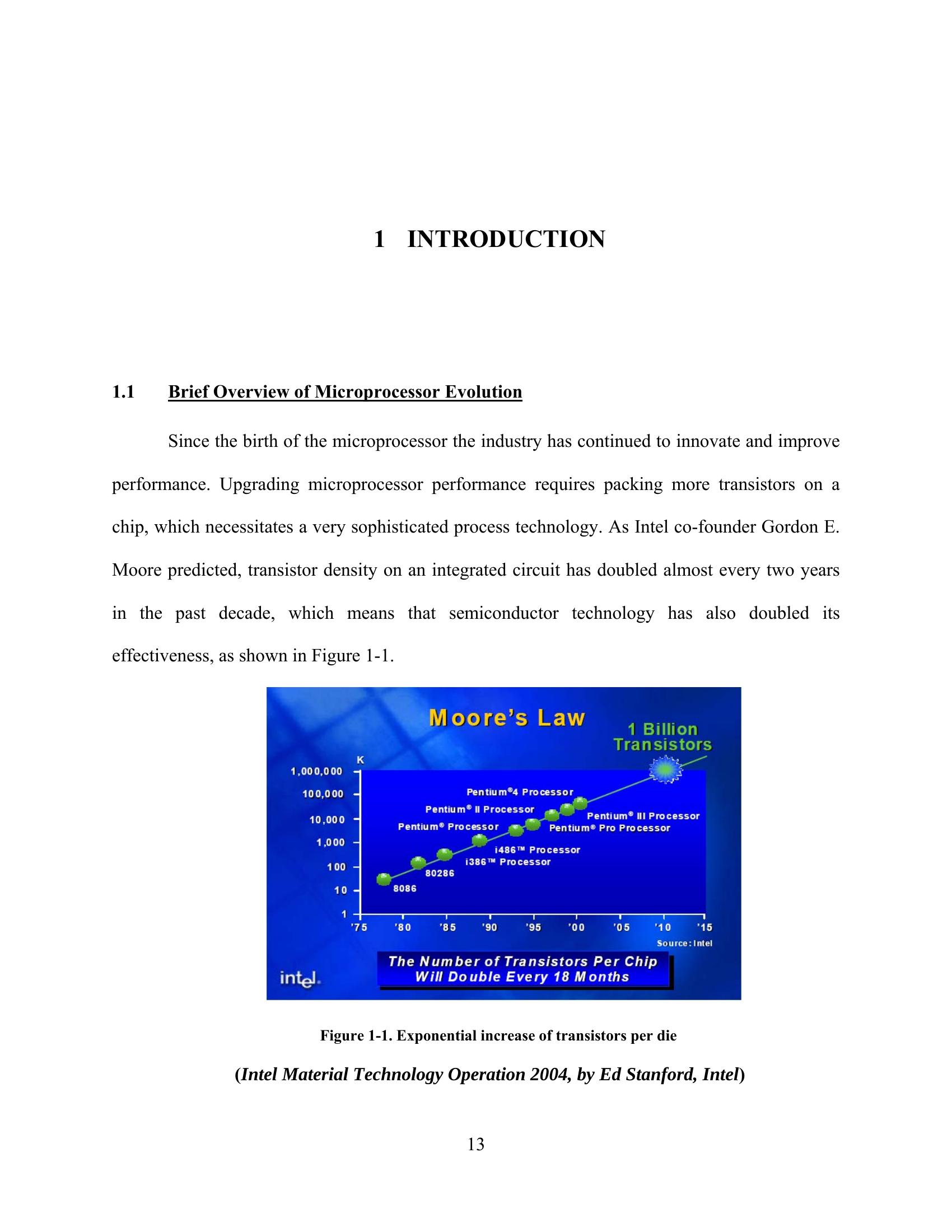
Since the birth of the microprocessor the industry has continued to innovate and improve
performance. Upgrading microprocessor performance requires packing more transistors on a
chip, which necessitates a very sophisticated process technology. As Intel co-founder Gordon E.
Moore predicted, transistor density on an integrated circuit has doubled almost every two years
in the past decade, which means that semiconductor technology has also doubled its
effectiveness, as shown in Figure 1-1.
Figure 1-1. Exponential increase of transistors per die
(Intel Material Technology Operation 2004, by Ed Stanford, Intel)
13
The microprocessor frequency of operation has also increased dramatically along with
the increase of device density. Load transition speeds have also increased as a result of high
frequencies. Billions of transistors operating in GHz scale frequencies result in tremendous
amount of power dissipation leading to very high overall and extremely high-localized spatial
thermal stress. As a consequence, there is an immediate need for techniques to manage power
and performance especially in systems that run multiple applications such as multi-core systems.
With the recent trend towards system-on-a-chip and multi-core systems, power management
techniques that were designed for single-core microprocessors must be improved and applied at
the chip-level to exploit the larger design space.
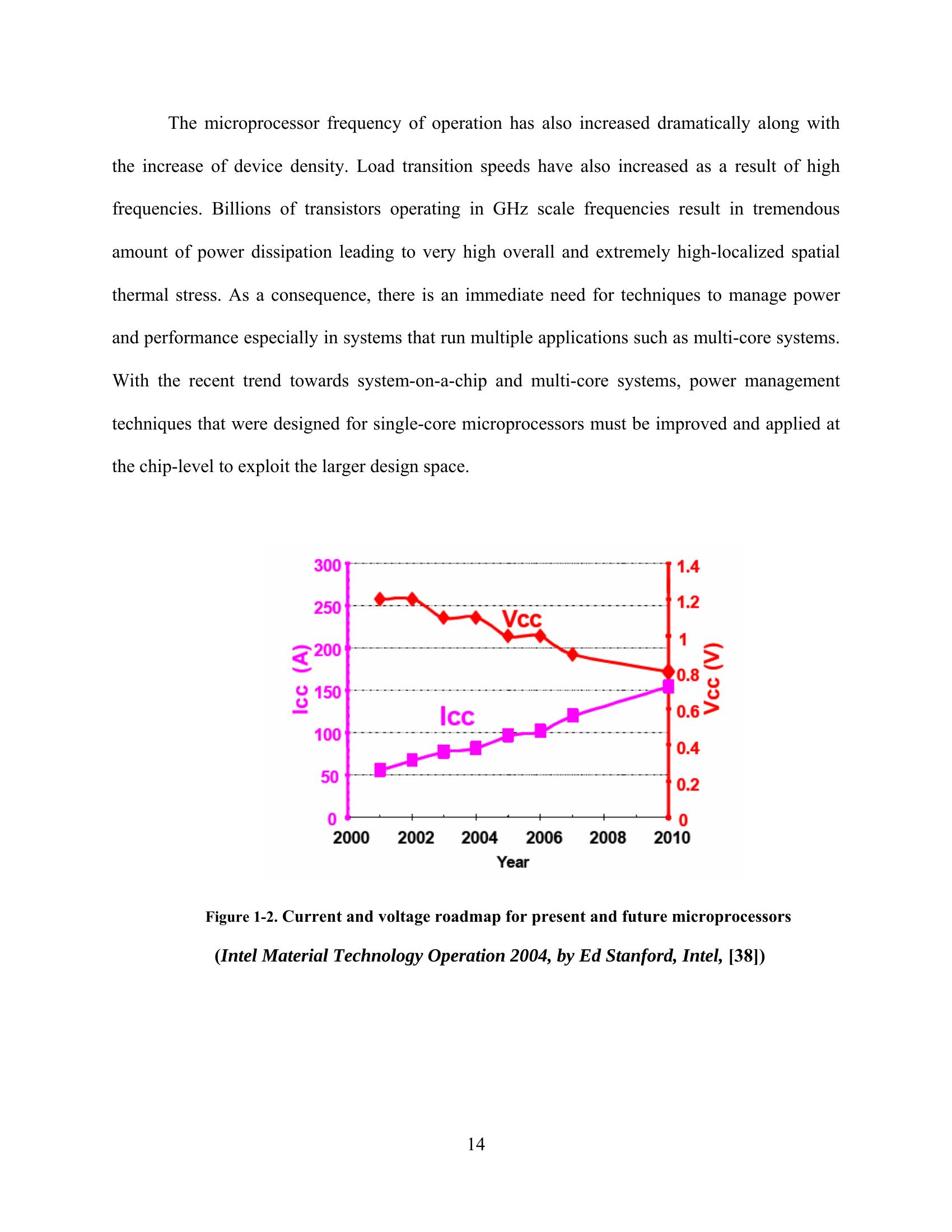
Figure 1-2. Current and voltage roadmap for present and future microprocessors
(Intel Material Technology Operation 2004, by Ed Stanford, Intel, [38])
14
1.2 Microprocessor Power Delivery and Load Characteristics
As users demand each generation of devices to handle more complex tasks, higher levels
of computation and performance are required [1]. Technology scaling has continuously driven
towards higher levels of integration, higher frequencies, higher currents, and lower operating
voltages, as shown in Figure 1-2. Current demands have increased with the number of
transistors, and in order to keep the power consumption low, the supply voltage has decreased.
System architecture is also changing with rapidly scaled technology [21] and power/performance
tradeoffs will be made visible to chip architects [28]. For technologies down to 90 nm it has been
possible to continue increasing performance while reducing power for the same functionality
from one processor generation to the next. However, for 65 nm and below, the effect of
increased interconnection length and resistance, coupled with a relatively flatter operating
voltage, has caused a significant dynamic and static power increase in complex chips [13].
Due to these factors (low voltage, high current, and fast load transition speeds) delivering
high-quality power to modern processors has become a challenging task. Few years ago CMOS
processors used to operate with frequencies above 300MHz with 2.5-3.3V output range but
future processors will be designed at 1.1V-1.8V range in order to improve their speed and power
performance [23]. As a result they will introduce dynamic loads with high current slew rates
during transients, and therefore, it is no longer practical to provide power to these processors
directly from the supply.
A special power supply device, the voltage regulator, with high efficiency and fast
transient response is needed to deliver the required high current and well-regulated voltage in
very fast transient response conditions. Voltage regulators that are integrated on the same chip as
the core provide the benefit of per-core voltage control and fast-voltage switching [2]. Since the
15
processor’s operating voltage is much lower than the supply voltage, a step-down voltage
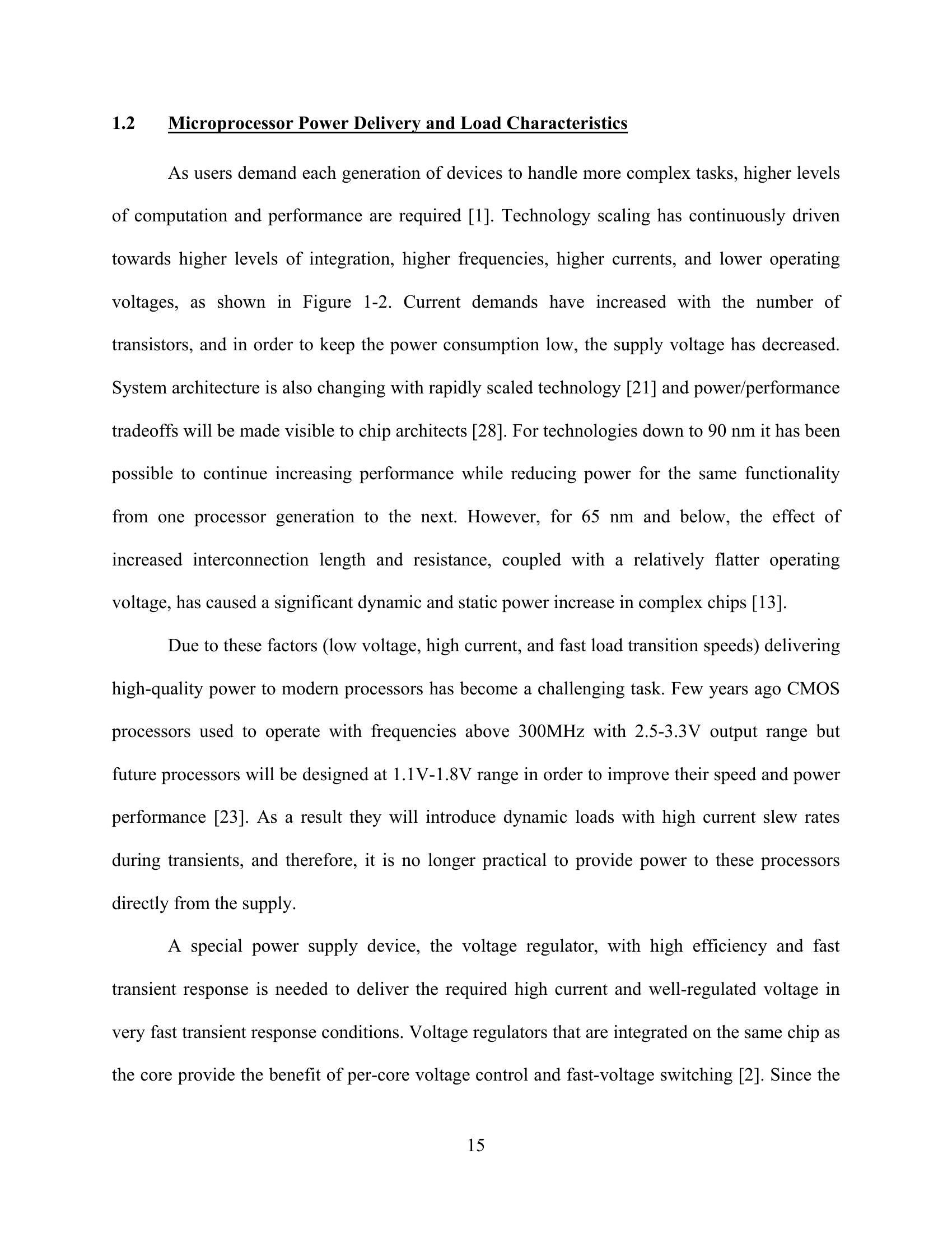
regulator module (VRM) is needed. Figure 1-3 shows the conceptual power delivery of a
microprocessor, employing a DC/DC step-down voltage regulator module (VRM) that is needed
to deliver power from the source to the load and to provide constant voltage. In addition, the
voltage regulator controls power fluctuations, and prevents damages to loads connected to the
supply.
Figure 1-3. Voltage regulator providing power to the microprocessor
There are two types of voltage regulators that are used to provide power to the processor,
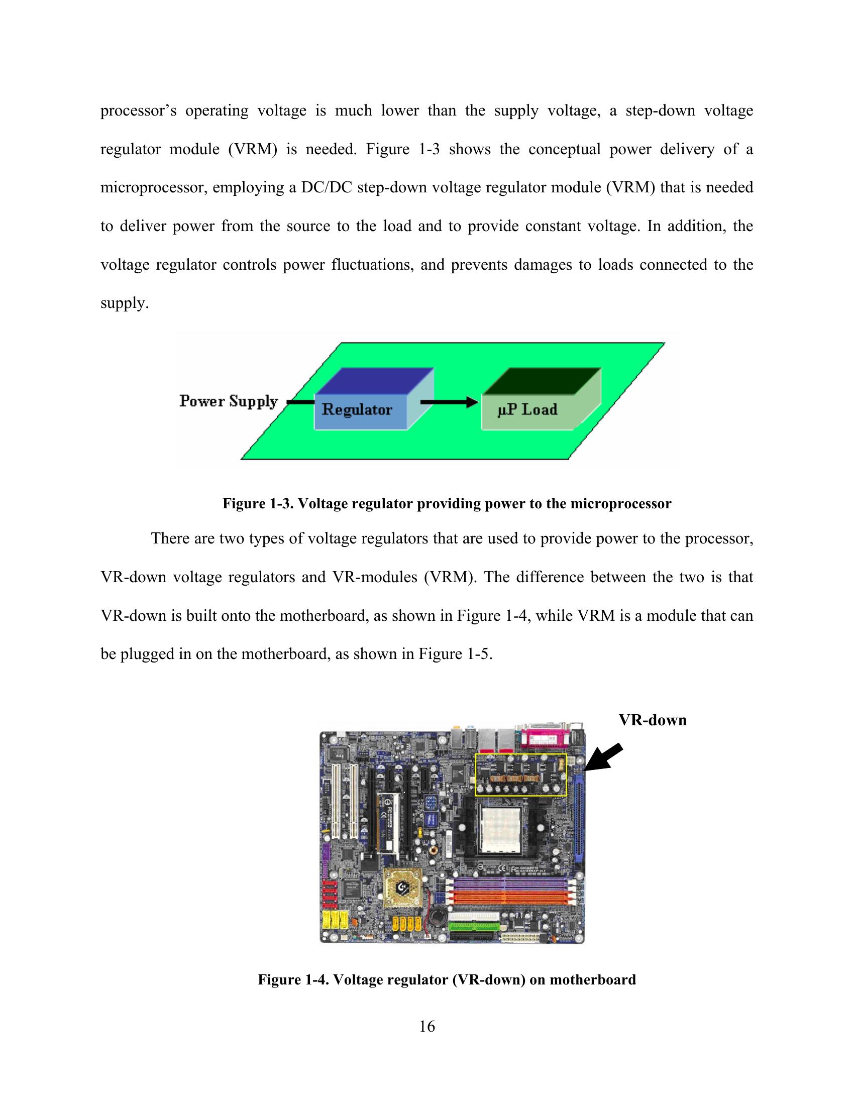
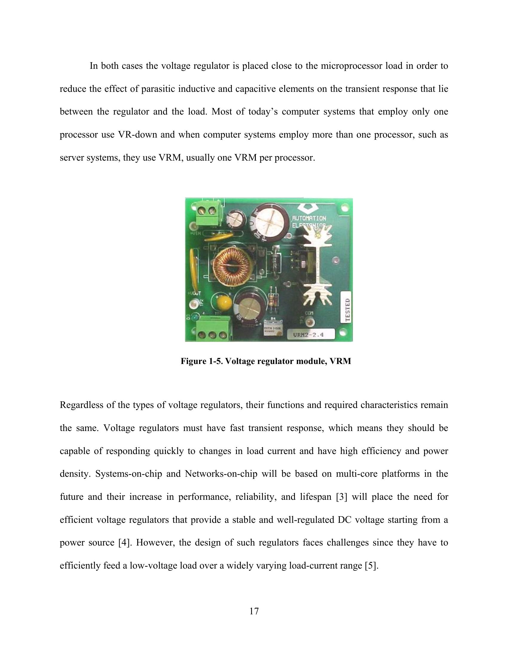
VR-down voltage regulators and VR-modules (VRM). The difference between the two is that
VR-down is built onto the motherboard, as shown in Figure 1-4, while VRM is a module that can
be plugged in on the motherboard, as shown in Figure 1-5.
VR-down
Figure 1-4. Voltage regulator (VR-down) on motherboard
16
In both cases the voltage regulator is placed close to the microprocessor load in order to
reduce the effect of parasitic inductive and capacitive elements on the transient response that lie
between the regulator and the load. Most of today’s computer systems that employ only one
processor use VR-down and when computer systems employ more than one processor, such as
server systems, they use VRM, usually one VRM per processor.
Figure 1-5. Voltage regulator module, VRM
Regardless of the types of voltage regulators, their functions and required characteristics remain
the same. Voltage regulators must have fast transient response, which means they should be
capable of responding quickly to changes in load current and have high efficiency and power
density. Systems-on-chip and Networks-on-chip will be based on multi-core platforms in the
future and their increase in performance, reliability, and lifespan [3] will place the need for
efficient voltage regulators that provide a stable and well-regulated DC voltage starting from a
power source [4]. However, the design of such regulators faces challenges since they have to
efficiently feed a low-voltage load over a widely varying load-current range [5].
17
1.3 The Role and Operation of a Voltage Regulator
The role of the voltage regulator is to deliver power from the source, which is usually
unregulated, to the load, which needs regulated voltage [36] with minimum loss and maintain
constant voltage to the microprocessor during transient response. Changes in load current occur
when the microprocessor switches between sleep mode and active mode, and vice versa. When
load currents increase step up transients occur and when load currents decrease step down
transients occur. Since there are a large number of transistors involved, the microprocessor
performs fast transitions between different load levels, which need to be completed quickly due
to high clock speeds. These performance constraints along with power density and efficiency
concern voltage regulator design.
In recent years, low voltage-power converters are achieving remarkable attention because
the most effective way to reduce the power of active circuits is by operating at a lower power
supply voltage ([39], [49]). High-efficiency converters are necessary for smooth power delivery
and handling of load variation. There would be large power dissipation, which would result in
heat, and therefore, large and expensive cooling systems would be needed. The efficiency of a
converter having output power, P and input power, P is:
OUT IN
η = P /P (1-1)
OUT IN
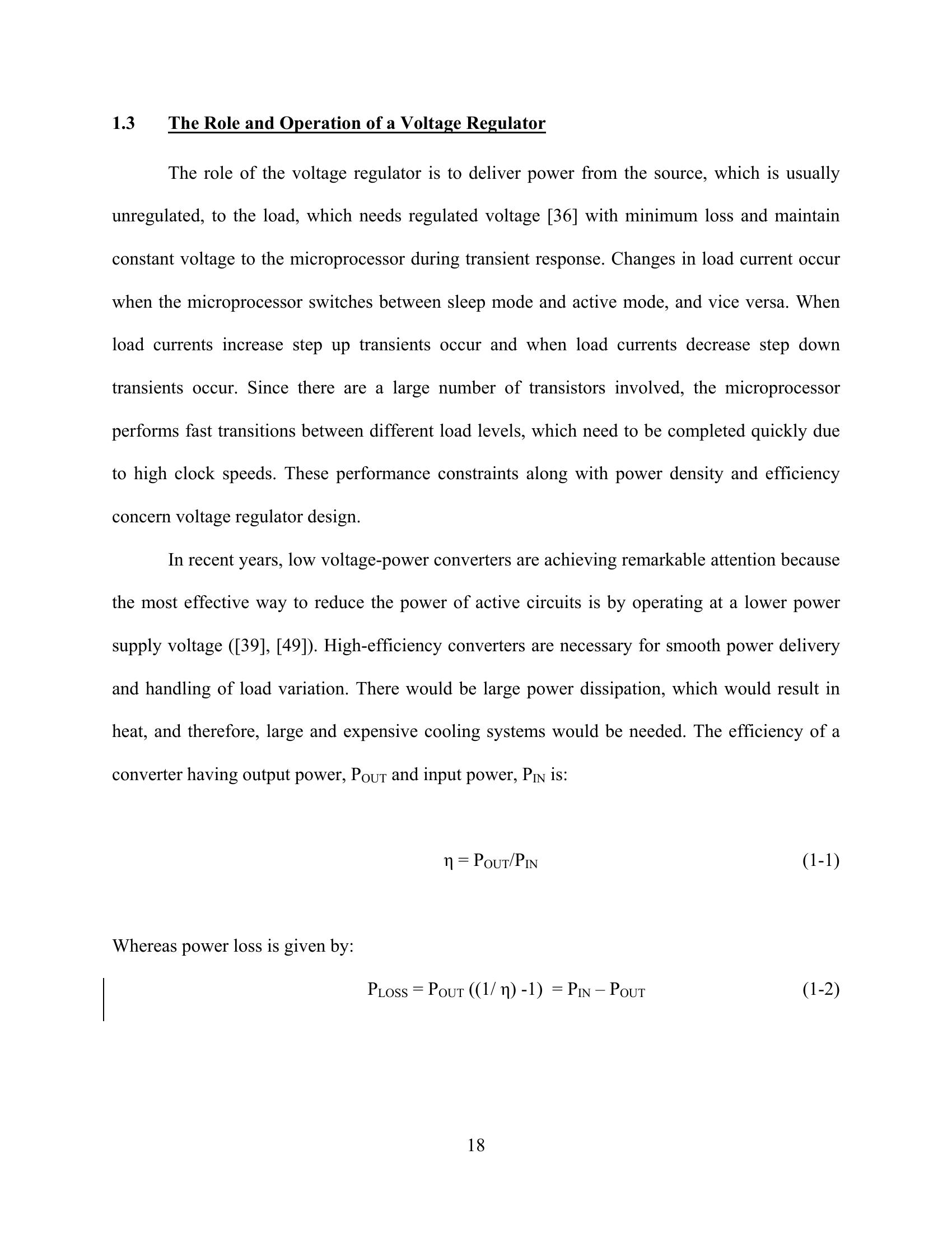
Whereas power loss is given by:
P = P ((1/ η) -1) = P – P (1-2)
LOSS OUT IN OUT
18
This power loss is converted into heat, which must be removed from the converter. This leads to
a large and expensive cooling system, it causes the electronic elements within the converter to
operate at high temperature, and it reduces the system reliability. Certainly, at high output
powers, it may be impossible to sufficiently cool the converter elements using current
technology.
Efficiency is a good measure of the quality of a given converter technology. When very
little power is lost, the converter elements can be packaged with high density, leading to a
converter of small size and weight, and of low temperature rise. The question is how can we
build a converter circuit that changes the voltage, yet dissipates negligible power? The available
circuit elements that can be used to build such converter circuit are [51]:
• Resistive elements, capacitive elements, magnetic devices including inductors and
transformers, semiconductor devices operated in the linear mode (for example, as
class A or class B amplifiers)
• Semiconductor devices operated in the switched mode (such as in logic devices
where transistors operate in either saturation or cutoff).
Unregulated Semiconductor Regulated
LOAD
Voltage Switches Voltage
Control
Figure 1-6. Voltage regulator operation
19
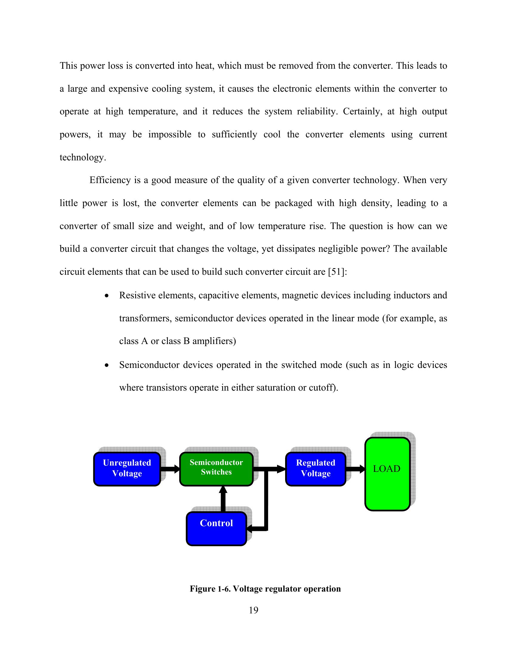
Figure 1-6 shows how the voltage regulator takes an unregulated voltage and through
semiconductor switches and control circuitry provides a regulated output voltage that is suitable
for load operation.
In conventional signal processing applications, where efficiency is not the primary
concern, inductors are usually avoided wherever possible, because of their large size and the
difficulty of incorporating them into integrated circuits. In contrast, capacitors and magnetic
devices are important elements of switching converters, because ideally they do not consume
power. It is the resistive element, as well as the linear-mode semiconductor device, that is
avoided [2]. Switched-mode semiconductor devices are also employed. When a semiconductor
device operates in the off state, its current is zero, and hence its power dissipation is zero. When
the semiconductor device operates in the on (saturated) state, its voltage drop is small, and hence
its power dissipation is also small. In either event, the power dissipated by the semiconductor
device is low. So capacitive and inductive elements, as well as switched-mode semiconductor
devices, are available for synthesis of high-efficiency converters.
1.4 Off-Chip VR Alernatives
There are various types of voltage regulators that can be used for off-chip implementation
on the motherboard. The selection of the regulator topology depends upon system requirements
for maximum load current, output voltage tolerance, quiescent current, type of input voltage
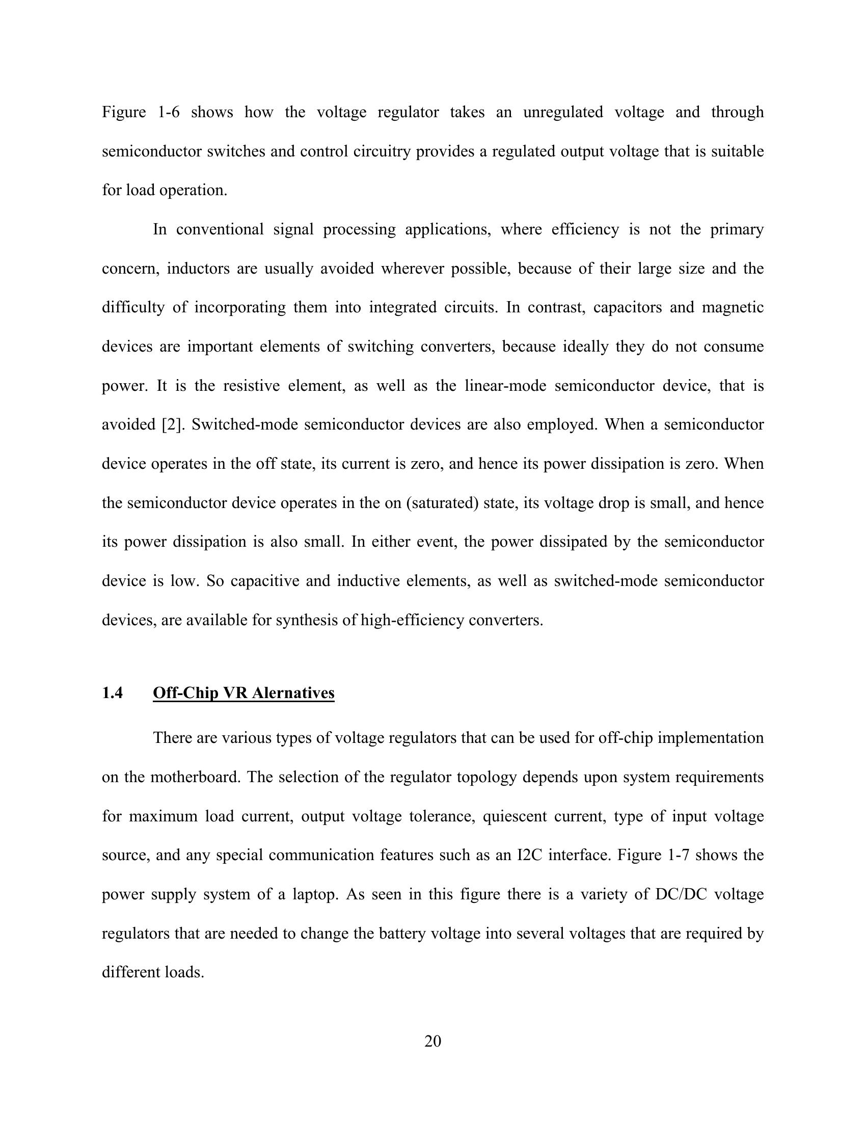
source, and any special communication features such as an I2C interface. Figure 1-7 shows the
power supply system of a laptop. As seen in this figure there is a variety of DC/DC voltage
regulators that are needed to change the battery voltage into several voltages that are required by
different loads.
20
Display
Inverter
Backlighting
Buck Microprocessor
AC Charger
Boost Disk
Drive
Figure 1-7. Laptop power supply
In this scheme, the charger converts alternating current (AC) from the power line to
direct current (DC) to charge the battery. The inverter produces high voltage and high frequency
AC that is needed to drive lamps for backlighting. The boost converter is a step-up converter
which increases battery voltage to the level required by the disk drive. Finally, the buck
converter which is a step-down converter decreases battery voltage to produce low level DC
voltage that is needed by the microprocessor. Here, the microprocessor requires aggressive
power management to control various modes such as sleep mode and active mode in order to
reduce power consumption and save battery life.
Despite the variety of voltage regulators that were mentioned for motherboard
application, our main focus will be the buck converter since its design and implementation is
crucial in delivering power to the microprocessor. A fundamental circuit for buck converter is
shown in Figure 1-8 and a synchronous buck converter is shown in Figure 1-9.
21
| None | |
| None |
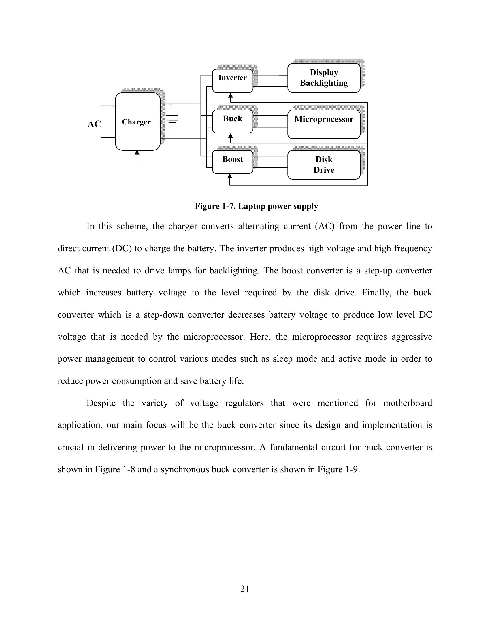
Figure 1-8. Circuit of a conventional buck converter [23]
Figure 1-9. Circuit of a synchronous buck converter [33]
Low-voltage power supplies require a synchronous buck converter as oppose to the conventional
converter. Here, the diode is replaced by a MOSFET for better efficiency. The transistor channel
conducts current in the reverse direction and blocks negative voltage while conducting positive
current. The diode is the major source of loss and when it is replaced by MOSFET the
conduction loss decreases since the transistor operates as a synchronous rectifier. Other losses
include the series resistance of the battery, the on-resistance of the switching element, and the
resistances in the conductors, connectors and wiring [42, 43]. Switching loss and inductance loss
increase with frequency, which limits the operating range of the DC-DC converters to a few
megahertz (1, [46]). Another buck converter topology that is typically used on the motherboard
is the multi-phase buck, which consists of several phases in order to minimize the ripple of the
output current caused by the circuit inductor.
22
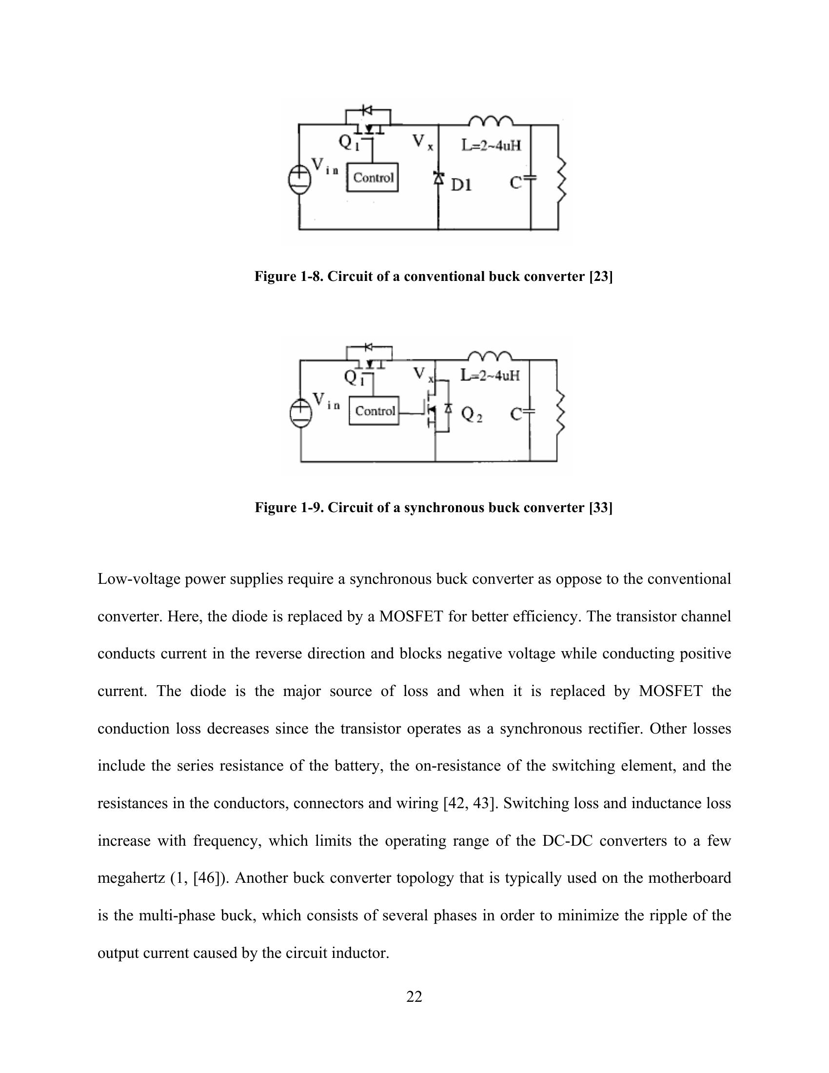
Figure 1-10. Circuit of a multi-phase buck converter [1]
Figure 1-10 shows a typical synchronous multi-phase buck converter that employs
inductances with smaller values. Large inductors cause large current ripple at the output so the
multi-phase buck converter allows the cancellation of the current ripples at the output node thus
providing an output current with less ripple. Using smaller inductances also improves transient
response and power density. Another potential benefit of this converter topology is the even
distribution of thermal dissipation due to scattering of the branches. Therefore, this technique has
become very popular in the power electronics industry. Drawback of this technique is that using
smaller inductance reduces efficiency [44].
1.5 Why On-Chip VR
In the recent years, the industry has been giving emphasis on integrating the voltage
regulators on the same chip as the load they feed. This will cause enormous benefits in multi-
core voltage regulation since on-chip integration will result in a decrease in size of filter
elements, which means higher operating frequencies, and thus will provide faster response to
changes in load current. Furthermore, on-chip implementation has potential to provide multiple
supply voltages in chip multiprocessor systems.
23
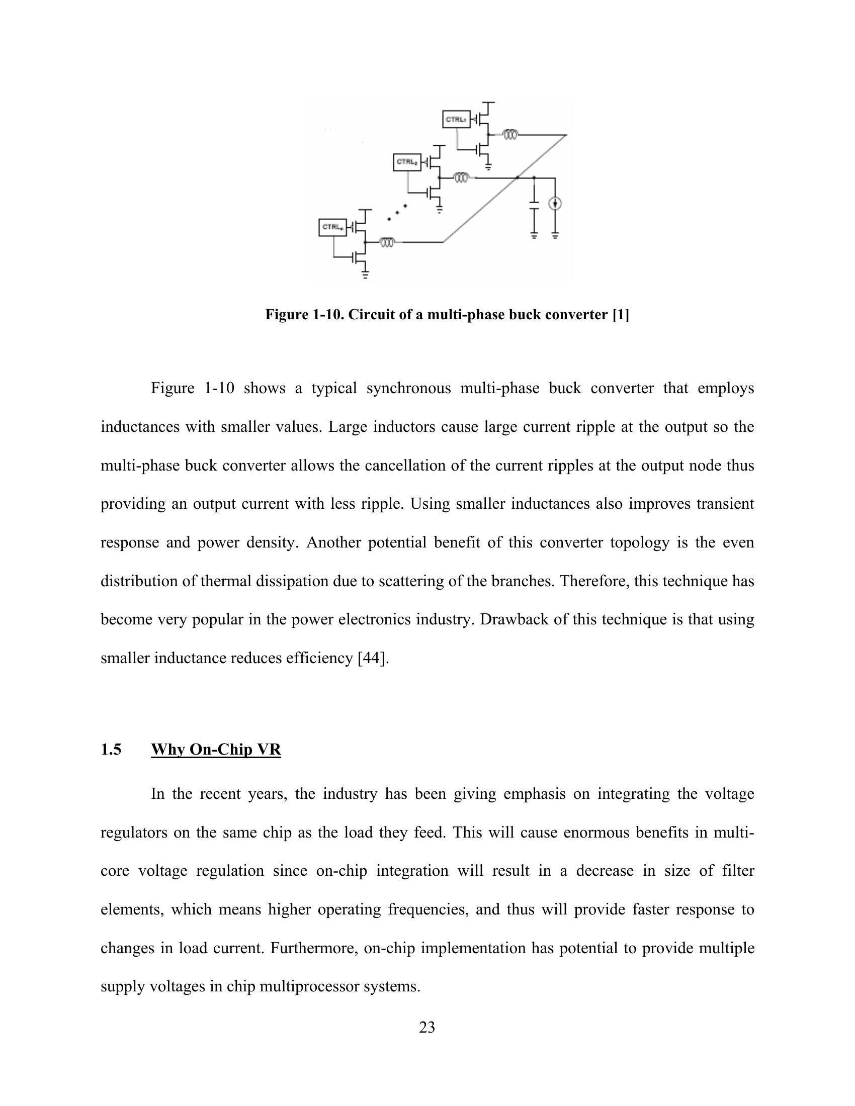
1.5.1 Limitations of Off-Chip Voltage Regulator
Voltage regulators deliver power from an energy source to multiple integrated circuits.
They are typically off-chip devices due to the large power transistors and output filter
components that are required. However, these off-chip regulators occupy a significant portion of
the PCB area and make it costly. Furthermore, off-chip voltage regulators operate at low
frequencies, which prevent them from adjusting to new voltages rapidly. Also, there are parasitic
elements (inductance and capacitance) in the power delivery network, between the VRM and the
load, which affect the voltage variation problem. Figure 1-11 shows a power delivery system
where the regulator is placed off-chip and as a result it cannot respond quickly to changes in load
current. Also, since the parasitic components reside between the load and the regulator, they will
create resonance in the circuit.
Resonance
Figure 1-11. Off-chip voltage regulator module [1]
In order to minimize this effect, voltage regulators can be placed close to the load. However,
the drastic load current change (di/dt) problem in processors and mid-frequency package
resonance issues cannot be eliminated. Decoupling capacitors can be added on the PCB to reduce
this effect; but even this is not the optimal solution since placing many capacitors on the PCB
occupies valuable area.
24
1.5.2 Limitations of Off-Chip Voltage Regulator
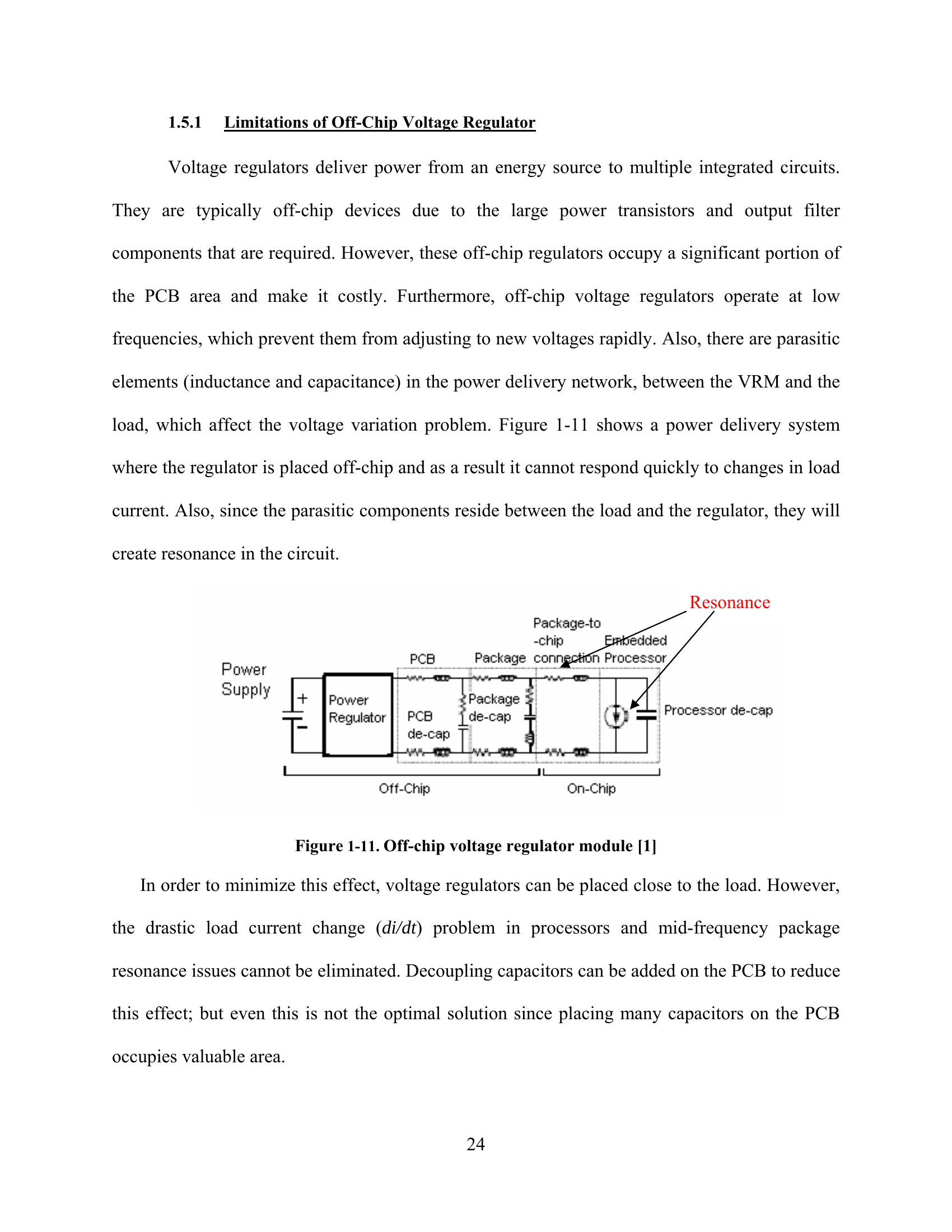
On-chip regulators provide faster voltage switching and improved power delivery. They
remove impedance restrictions of the power delivery systems by reducing mid-frequency
package resonance issues. Furthermore, an on-chip regulator operating at high switching
frequencies avoids bulky filter components such as inductors and capacitors, allows filter
capacitor to be integrated entirely on-chip, and enable fast voltage transients.
Figure 1-12. On-chip voltage regulator module [1]
With the growing push towards multi-core system-on-chip implementations, in recent years,
there has been a surge of interest to build on-chip integrated switching voltage regulators [9, 10].
Tight integration between the VR and the microprocessor results in resonance elimination. These
regulators, operating with high switching frequencies, can obviate large valued inductors and
capacitors, allow the filter capacitor to be integrated entirely on-chip, place smaller inductors on
the package, and enable fast voltage transitions at nanosecond timescales [2]. There is a direct
tradeoff between the switching frequencies of the voltage regulator and their power conversion
efficiency [2].
25
1.6 Thesis Outline
This dissertation consists of six chapters, which are organized as follows. Chapter 1 is the
background review of multiprocessor evolution and existing voltage regulator topologies that are
used both off-chip and on-chip. Motivation of this dissertation as well as various limitations and
benefits of present on- and off-chip regulator topologies are also discussed. Chapter 2 offers a
detailed discussion and survey of regulator topologies that have been used for on-chip
implementation, as well as it discusses their benefits and drawbacks. Chapter 3 includes on-chip
regulator options for integrating a hot swap controller on-chip along with a switching regulator to
control and protect the core from seeing any droops in the circuit. Chapter 4 is the two-stage tree
design technique that is proposed to deliver power to various function blocks in a system-on-
Chip. Simulations and analysis are performed to show that this technique provides high
efficiency and is suitable for system-on-chip implementation. Chapter 5 includes a proposal for
system-on-chip and multi-core systems and why the proposed hybrid technique is effective in
these environments, detailed discussion of our future work is also discussed. Finally Chapter 6
concludes the dissertation.
26
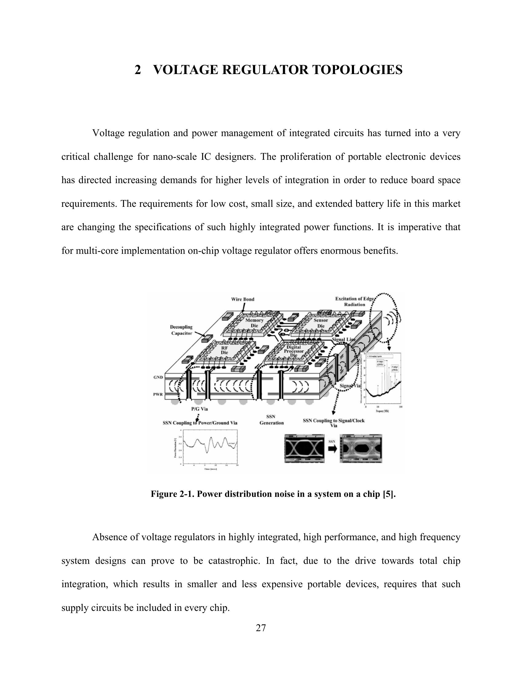
2 VOLTAGE REGULATOR TOPOLOGIES
Voltage regulation and power management of integrated circuits has turned into a very
critical challenge for nano-scale IC designers. The proliferation of portable electronic devices
has directed increasing demands for higher levels of integration in order to reduce board space
requirements. The requirements for low cost, small size, and extended battery life in this market
are changing the specifications of such highly integrated power functions. It is imperative that
for multi-core implementation on-chip voltage regulator offers enormous benefits.
Figure 2-1. Power distribution noise in a system on a chip [5].
Absence of voltage regulators in highly integrated, high performance, and high frequency
system designs can prove to be catastrophic. In fact, due to the drive towards total chip
integration, which results in smaller and less expensive portable devices, requires that such
supply circuits be included in every chip.
27
2.1 Complete Survey of all On-Chip VRM Topologies
Key to the design of power efficient ICs is performing high-efficiency DC/DC
conversion. In general, DC/DC converters are placed off-chip, where one regulator resides
between the source and each load and this is called star configuration [25]. This regulator
delivers current with the appropriate voltage levels to different loads in the circuit. ITRS predicts
an increase in the power consumption of microprocessors for future applications. The power
delivery network (PDN) provides the power supply to the processors and when it is not designed
properly it may be a major source of noise in the circuit, especially in high-speed electronic
systems.
2.1.1 Linear Regulators
The linear regulator is the fundamental building block of almost every power supply used in
electronics. It offers ease of on-chip implementation due to its small size, low cost, low noise, no
complexity and fast response to load current transients. Furthermore, since the linear regulators
are inexpensive and small in size they provide enormous benefits in systems requiring multiple
voltage islands.
Figure 2-2. Linear regulator
28
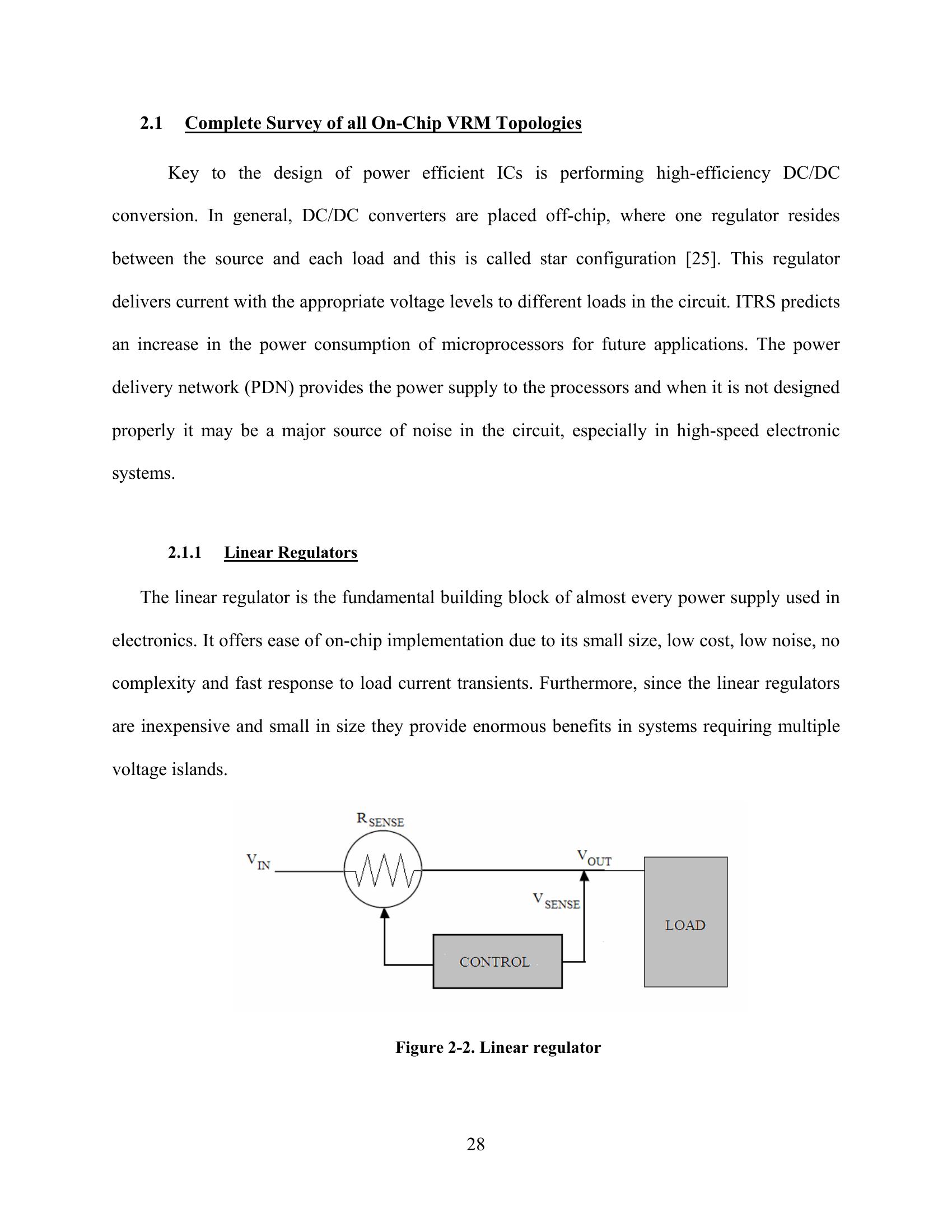
Typical linear regulator is shown in Figure 2-2. The low noise characteristics and smaller size
and complexity also makes them potential candidates in systems where the difference between
the input and output voltages is small. This topology is especially preferred in low power
applications due to their low quiescent currents.
Referring to Figure 2-2, the linear regulator operates using a MOSFET acting as a sense
resistor in order to force a fixed voltage at the output. The role of the control circuit is to monitor
the output voltage and adjust the current through the sense resistor so the output voltage is held
at the desired value. The most efficient form of a linear regulator is the low dropout (LDO) linear
regulator. The dropout voltage refers to the minimum voltage drop required across the regulator
to maintain output voltage regulation. The lower the dropout voltage is, the higher its power
efficiency is since there is maximum power delivered to the load, which is given by:
P = (V V )*I (1-3)
IN- dropout load
Power extracted from the input source is:
P = V *(I + I ) (1-4)
IN load quiescent
P = (V -V )*I (1-5)
OUT IN load
Iquiesecent is the quiescent current in the internal LDO circuitry. To have a high efficiency LDO
regulator the dropout voltage and the quiescent current must be minimized and also, the voltage
29
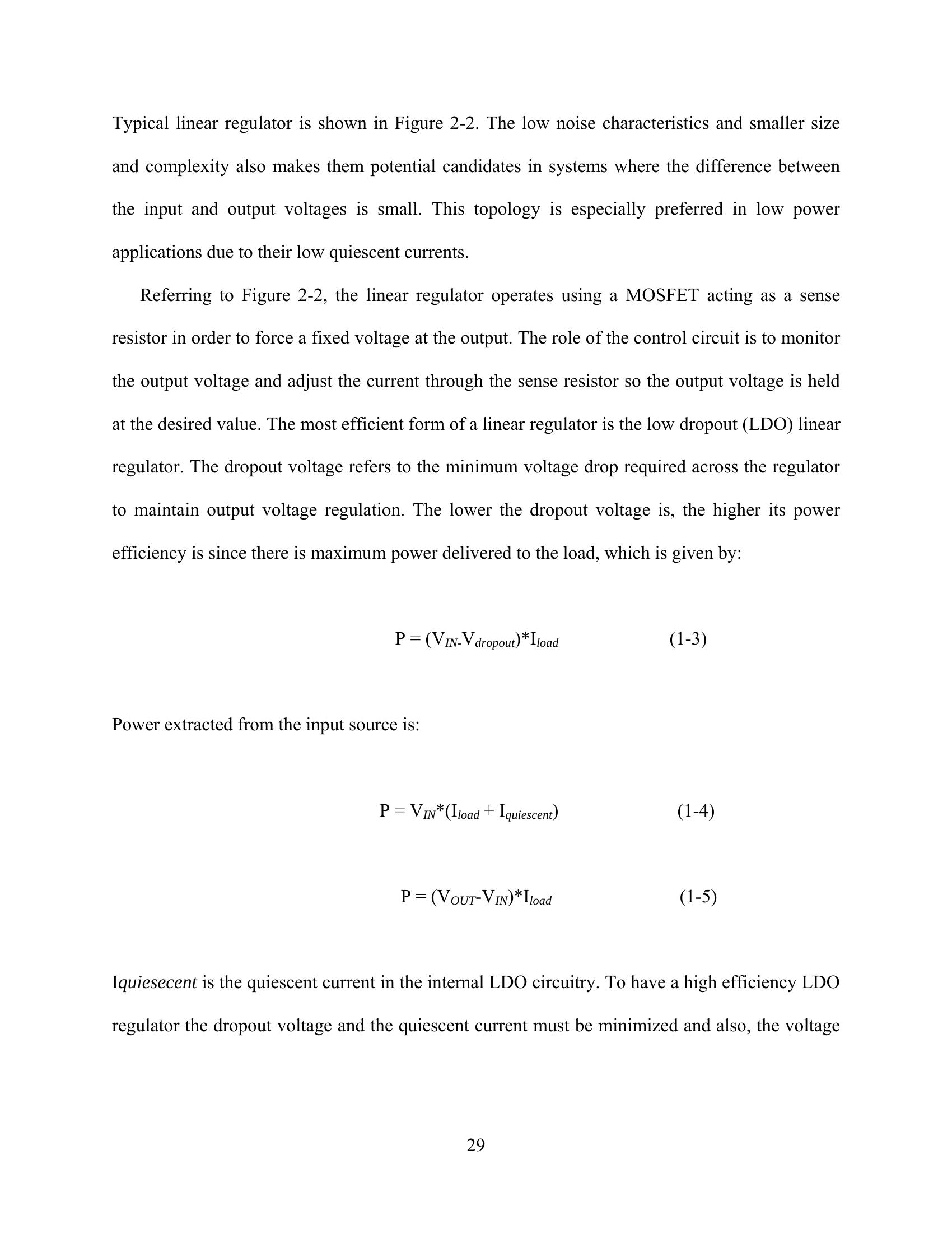
difference between input and output must be minimized since the internal power dissipation of
LDO regulators, equation (1-5) accounts for the loss of power efficiency.
2.1.2 Switching Regulators
Switching regulators are generally mixed-mode circuits that feed back an analog error
signal and digitally gate it to provide bursts of current at the output [29]. They provide good
power conversion efficiency due to the presence of inductor, which is a low-loss energy transfer
device. This regulator topology is less sensitive to the V /V ratio and can regulate a wide
OUT IN
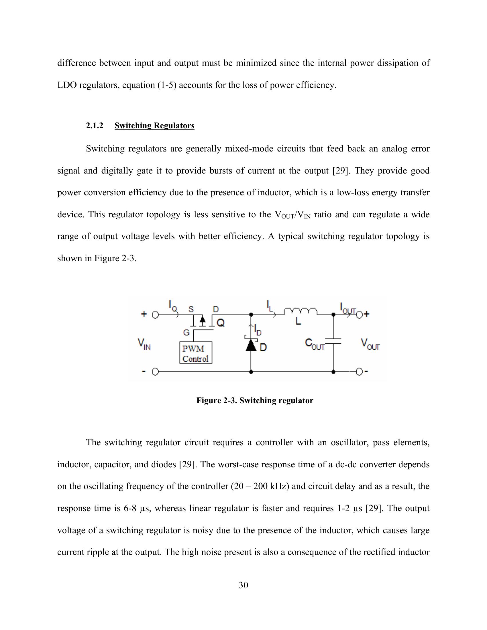
range of output voltage levels with better efficiency. A typical switching regulator topology is
shown in Figure 2-3.
Figure 2-3. Switching regulator
The switching regulator circuit requires a controller with an oscillator, pass elements,
inductor, capacitor, and diodes [29]. The worst-case response time of a dc-dc converter depends
on the oscillating frequency of the controller (20 – 200 kHz) and circuit delay and as a result, the
response time is 6-8 µs, whereas linear regulator is faster and requires 1-2 µs [29]. The output
voltage of a switching regulator is noisy due to the presence of the inductor, which causes large
current ripple at the output. The high noise present is also a consequence of the rectified inductor
30
voltage behavior of the output of these converters. Also, the noise problem is aggravated by
on/off sleep mode transitions.
2.2 Other On-Chip-Friendly VR Topologies
There are other topologies that may be used for on-chip implementation however their
use is limited by system requirements and specifications.
2.2.1 Switched Capacitor Circuits (Charge Pumps)
This type of DC/DC converters consist of switches and energy transfer capacitors in the
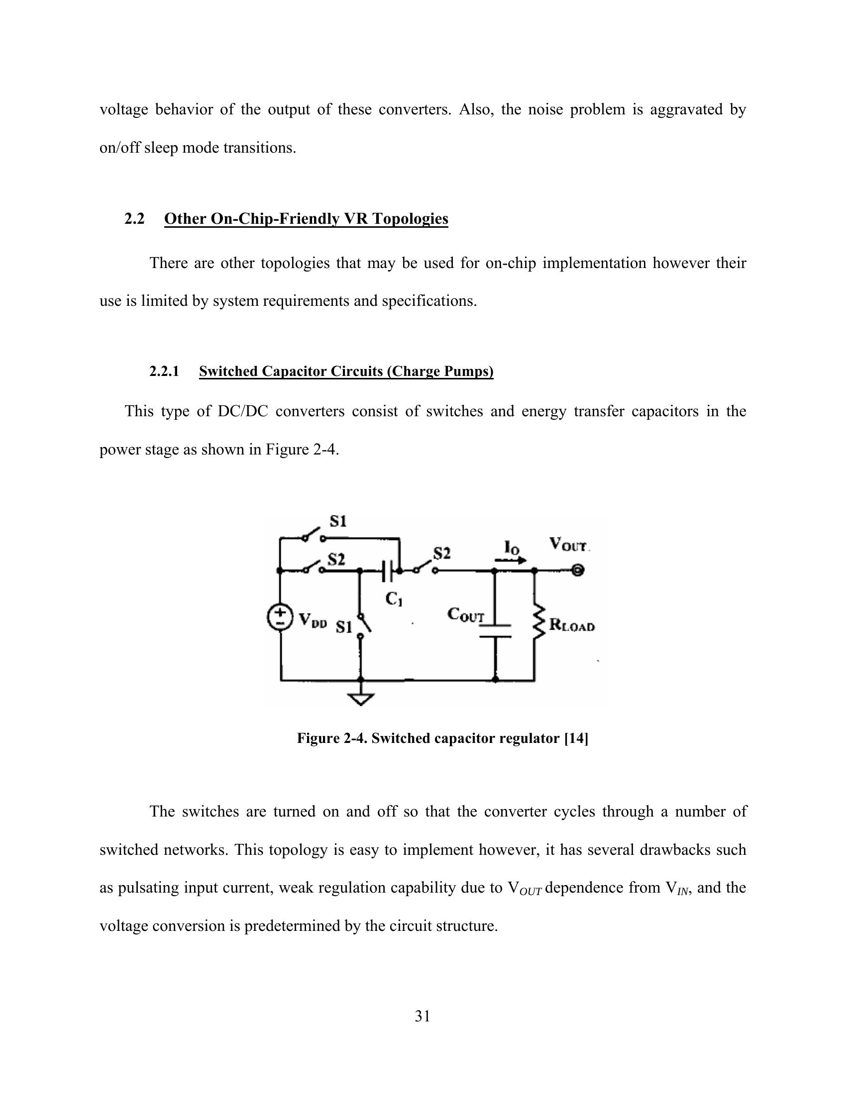
power stage as shown in Figure 2-4.
Figure 2-4. Switched capacitor regulator [14]
The switches are turned on and off so that the converter cycles through a number of
switched networks. This topology is easy to implement however, it has several drawbacks such
as pulsating input current, weak regulation capability due to V dependence from V , and the
OUT IN
voltage conversion is predetermined by the circuit structure.
31
2.2.2 MEMS Approach (DC/DC Converters with MEMS Inductors)
MEMS technology provides the integration of passive elements on-chip. These types of
DC/DC converters use micro-machined inductors. However, major drawback of this technique is
process compatibility with fabrication processes. It is very difficult to interface these types of
DC/DC converters on-chip with CMOS or BJT devices.
2.2.3 Inductor Multiplier Technique
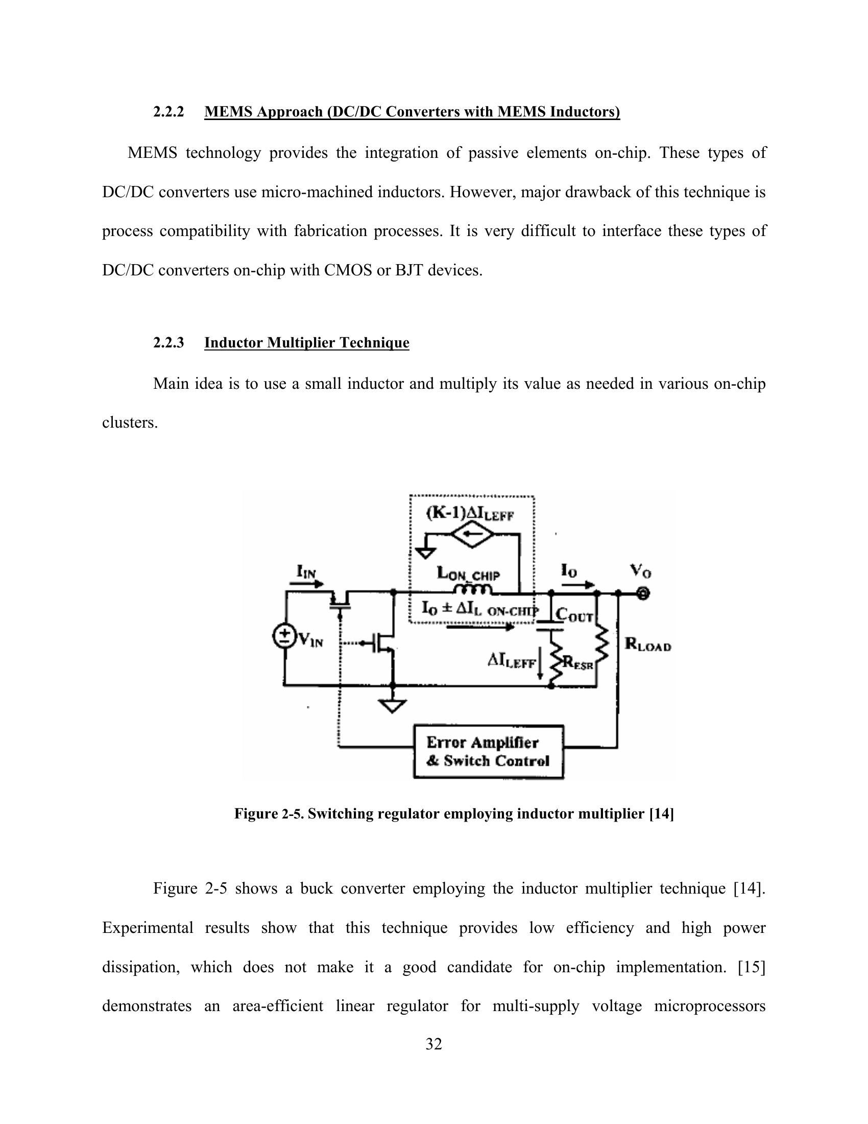
Main idea is to use a small inductor and multiply its value as needed in various on-chip
clusters.
Figure 2-5. Switching regulator employing inductor multiplier [14]
Figure 2-5 shows a buck converter employing the inductor multiplier technique [14].
Experimental results show that this technique provides low efficiency and high power
dissipation, which does not make it a good candidate for on-chip implementation. [15]
demonstrates an area-efficient linear regulator for multi-supply voltage microprocessors
32
implemented in a 90 nm CMOS technology. This approach is good in terms of achieving high
current efficiency of 94%, however, it only provides 74% power efficiency for a 1.2V input and
0.9V output. Efficiency in the case of linear regulators is sensitive to V /V ratio. [16] also
OUT IN
provides an on-chip linear regulator topology that exhibits 96.5% current efficiency by
employing a flexible control technique of output current (FCOC). However, despite the high
current efficiency, power efficiency is relatively low for a 5V input and 3V output. It is about
60% due to the V /V dependency. An on-chip, two-stage approach consisting of a switched
OUT IN
capacitor regulator for high-voltage conversion and a linear regulator for low voltage conversion
was demonstrated in [50] however, this approach provides low efficiency.
2.3 Relative Merits/Demerits of Each Option
The integration of voltage regulators on the same chip that needs to be supplied poses
new challenges on process technology. This means that these regulators need to be available in
the same process technology as the application. It is very difficult to accomplish this task while
maintaining high efficiency and system performance. Both preferred topologies, linear and
switching, for on-chip implementation pose significant demerits in this concern.
Starting with the linear regulator, its dependency on the V /V ratio has negative
OUT IN
impact on the efficiency. If the value of the output voltage, V , is close to the value of the
OUT
input voltage, V , such as V /V = 1.0V/1.1V = 90% efficiency, we get good efficiency.
IN OUT IN
However, if the output voltage is much lower than the input voltage, such as V /V = 5V/10V
OUT IN
= 50% efficiency, we get poor efficiency since we have to drop 5V across the regulator. If our
output current would be say 10A then power dissipation would be 10A*5V = 50W which cannot
33
be ignored when it comes to on-chip implementation. It requires heat sinks, which may increase
area and cost.
Next in line, switching regulators, also exhibit serious concerns when it comes to on-chip
implementation. Major drawback of this topology is the large size of the inductor and capacitor
that occupy large printed circuit board (PCB) area. So, for off-chip implementation these types of
regulators are good in terms of providing high-conversion efficiency, but they occupy valuable
PCB space. For on-chip implementation, the size of the inductor and capacitor is reduced since
the regulator operates at high frequencies. However, this results in efficiency degradation since
reducing the on-chip filter capacitor limits the total amount of instantaneous charge available to
the load thus causing voltage fluctuations [27]. Another drawback of on-chip switching
regulators is their lack of providing clean output voltage due to the presence of the inductor.
Ripple voltage needs to be low in order not to effect the operation of the circuit the regulator is
supplying to. The requirements for high efficiency and high accuracy make the size of the
inductor prohibitively large for SOC solutions, where the inductor is embedded in the chip.
2.4 On-Chip VRM Issues
Before unveiling the next two chapters that discuss proposed approaches for
microprocessor and system-on-a-chip power delivery and management by integrating the
regulator on the same chip as the application, we should point out the requirements and issues
that concern their on-chip implementation. On-chip implementation requirements are efficient,
small, inexpensive, and simple regulator topologies that besides providing constant and well-
regulated voltage should also be capable of allowing the creation of multiple voltage islands on-
34
chip. This is important given the technology trend towards system-on-chip and chip
multiprocessors. Some of the challenges include:
• Efficiency degradation due to size reduction of filter components and high switching
frequencies.
• Smaller capacitor provides less charge to the load, which becomes vulnerable to large
di/dt events that cause voltage fluctuations.
• In order to reduce fluctuations, decoupling capacitors are used but with the overhead
of increasing chip area.
• On-chip regulator uses the filter capacitor for both decoupling and filtering, which
causes large voltage droops since large load current steps rapidly drain out the limited
charge stored on the capacitor.
• Circuit droops are assisted by filter component size reduction.
• Inductance issues. A decrease in inductance size results not only in faster switching
and higher inductor ripple current, but in a more noticeable parasitic inductance in the
circuit as well.
• Inductor fabrication challenges.
35

3 ON-CHIP VRM FOR SINGLE AND DUAL CORE SYSTEMS
International Technology Roadmap for Semiconductors, ITRS, [11] as well as most other
studies and roadmaps have specified that in all future micro- and nano-electronic circuits and
systems power management and distribution will become the most serious design challenge.
Power consumption has a critical impact on IC performance and therefore its management is
important. Ineffective power management causes lower chip performance, increases area and
makes the design nonfunctional.
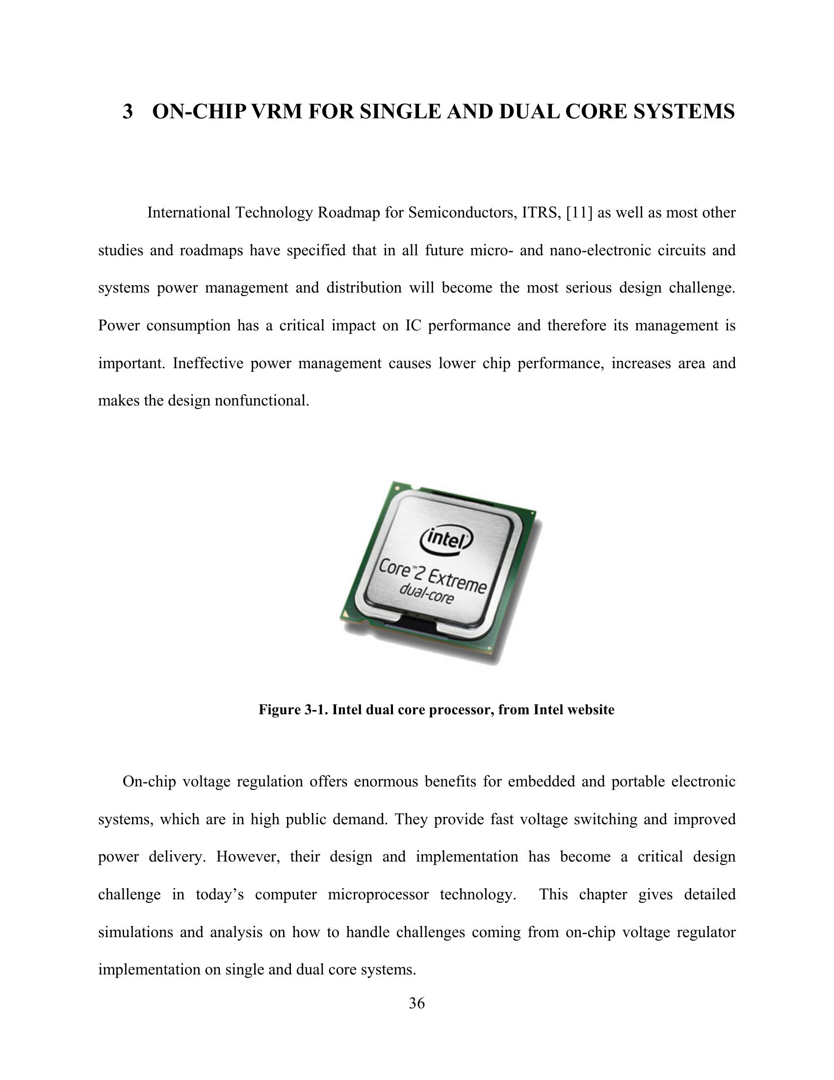
Figure 3-1. Intel dual core processor, from Intel website
On-chip voltage regulation offers enormous benefits for embedded and portable electronic
systems, which are in high public demand. They provide fast voltage switching and improved
power delivery. However, their design and implementation has become a critical design
challenge in today’s computer microprocessor technology. This chapter gives detailed
simulations and analysis on how to handle challenges coming from on-chip voltage regulator
implementation on single and dual core systems.
36
3.1 Single-Core Voltage Regulation
Voltage regulators are found in nearly all computing systems and are essential for
delivering power from an energy source to multiple integrated circuits at their respective, desired
fixed or time-varying voltage levels [2]. Every electronic system is designed to operate at some
nominal supply voltage. The role of the regulator in these systems is to provide this constant
voltage, control power fluctuations, and prevent damage to loads connected to the supply. The
selection of the IC voltage regulator depends upon system requirements for maximum load
current, output voltage tolerance, quiescent current, type of input voltage source, and any special
communication features such as an I2C interface. Voltage regulators are usually off-chip devices,
however, they tend to occupy large PCB area and provide slow response to changes in load
current. Recently, their on-chip implementation has been proposed.
Although there are a variety of voltage regulator topologies to choose from, the most
commonly used for on-chip implementation are linear and switching regulators. Linear
regulators offer good response to load current transients, ease of on-chip integration, they have
relatively small size, and they are less expensive [2]. Linear regulator designs provide a clean
output with very little noise, therefore they are more suitable to use in designs that require low
output noise and fast input-output reaction, since they provide good response to changes in load
current. Drawback of linear regulators is their efficiency degradation with the V /V ratio, as
OUT IN
well as their inability to step up voltage.
On the other hand, switching regulators offer higher power conversion efficiency due to
their low-loss external inductor and increased design flexibility. The inductor allows the
regulator to transfer energy from input to output with no loss and it filters the output from
switching signals. Furthermore, switching regulators generate multiple output voltages from a
37
single input voltage and operate as a switch where its duty cycle determines how much charge is
transferred to the load [1]. Different than linear regulators, some types of switching regulators,
such as boost regulators, can provide outputs that are higher than the input. Conventional
switching regulators operate at relatively low switching frequencies and utilize bulky filter
components such as inductors and capacitors [7, 8]. Hence, voltage regulator modules typically
are separate, board-level components, with slow voltage adjustment capabilities [2].
With the growing push towards total chip integration, in recent years, there has been a
surge of interest to build on-chip integrated switching voltage regulators [9, 10]. These
regulators, operating with high switching frequencies, can obviate large valued inductors and
capacitors, allow the filter capacitor to be integrated entirely on-chip, place smaller inductors on
the package, and enable fast voltage transitions at nanosecond timescales [2]. There is a direct
tradeoff between the switching frequencies of the voltage regulator and their power conversion
efficiency [2]. Despite the benefits offered by on-chip integration, there are also design
challenges that should be considered when placing voltage regulators on the same chip as the
load.
3.2 Buck-Type Switching Regulator for On-Chip Implementation
Since most of the circuit supply voltages are lower than the voltage of the primary source
to the board, such as the battery, switching regulators are used to step down the voltage [5].
Therefore, the most commonly used switching converter is the buck converter, shown in Figure
3-2. This converter topology uses an inverter that switches on and off and alternately connects
and disconnects the input voltage to the external inductor, which is connected to the output
terminal and its current is equal to the output current.
38
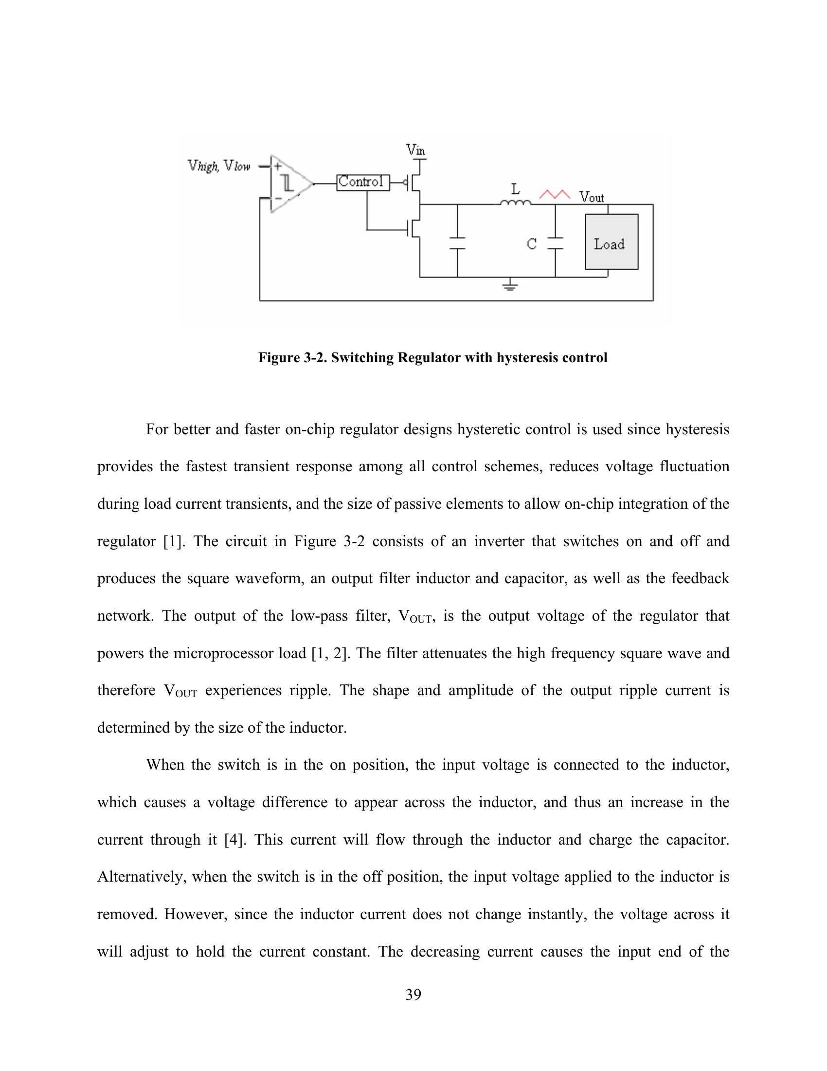
Figure 3-2. Switching Regulator with hysteresis control
For better and faster on-chip regulator designs hysteretic control is used since hysteresis
provides the fastest transient response among all control schemes, reduces voltage fluctuation
during load current transients, and the size of passive elements to allow on-chip integration of the
regulator [1]. The circuit in Figure 3-2 consists of an inverter that switches on and off and
produces the square waveform, an output filter inductor and capacitor, as well as the feedback
network. The output of the low-pass filter, V , is the output voltage of the regulator that
OUT
powers the microprocessor load [1, 2]. The filter attenuates the high frequency square wave and
therefore V experiences ripple. The shape and amplitude of the output ripple current is
OUT
determined by the size of the inductor.
When the switch is in the on position, the input voltage is connected to the inductor,
which causes a voltage difference to appear across the inductor, and thus an increase in the
current through it [4]. This current will flow through the inductor and charge the capacitor.
Alternatively, when the switch is in the off position, the input voltage applied to the inductor is
removed. However, since the inductor current does not change instantly, the voltage across it
will adjust to hold the current constant. The decreasing current causes the input end of the
39
inductor to have a negative voltage. This turns on the diode, and the inductor current flows
through the load and back through the diode. During the off state, the capacitor discharges into
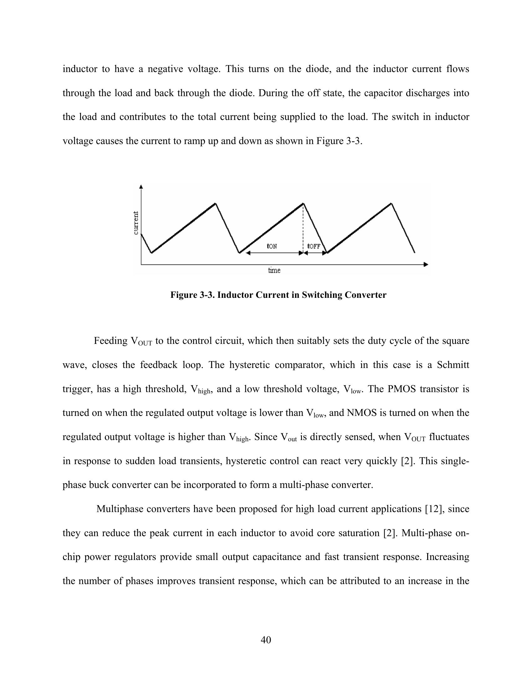
the load and contributes to the total current being supplied to the load. The switch in inductor
voltage causes the current to ramp up and down as shown in Figure 3-3.
Figure 3-3. Inductor Current in Switching Converter
Feeding V to the control circuit, which then suitably sets the duty cycle of the square
OUT
wave, closes the feedback loop. The hysteretic comparator, which in this case is a Schmitt
trigger, has a high threshold, V , and a low threshold voltage, V . The PMOS transistor is
high low
turned on when the regulated output voltage is lower than V , and NMOS is turned on when the
low
regulated output voltage is higher than V . Since V is directly sensed, when V fluctuates
high out OUT
in response to sudden load transients, hysteretic control can react very quickly [2]. This single-
phase buck converter can be incorporated to form a multi-phase converter.
Multiphase converters have been proposed for high load current applications [12], since
they can reduce the peak current in each inductor to avoid core saturation [2]. Multi-phase on-
chip power regulators provide small output capacitance and fast transient response. Increasing
the number of phases improves transient response, which can be attributed to an increase in the
40
effective switching frequency with more phases [1, 2]. However, large number of phases results
in large chip area, which is a major overhead introduced by this technique.
3.3 Implementation Challenges
Motivation for on-chip integration of voltage regulators is guided by increasing demand
for high-performance processor designs with improved power delivery networks. In addition, on-
chip integration saves PCB area and cost. When the regulator is placed close to the load, it
responds quicker to changes in load current thus resulting in fast voltage switching and also low
power microprocessor designs. However, there are many overheads associated with on-chip
integration and they need to be addressed. Since the regulator is moved on-chip the sizes of its
filter components are reduced. Smaller filter components result in higher switching frequencies,
which make the regulator less efficient. Also, a smaller capacitor size results in less charge
stored, which means less charge available to the load, which then introduces higher vulnerability
to large di/dt events that can cause large voltage fluctuations [1].
In order to reduce fluctuations, decoupling capacitors are used but with the overhead of
increasing chip area. A solution to this problem would be that the on-chip regulator uses the filter
capacitor for both decoupling and filtering. However, since the on-chip capacitor is much smaller
than the total decoupling and filter capacitance used for off-chip regulators, large load current
steps can rapidly drain out the limited charge stored on the capacitor before the regulator loop
can respond, resulting in a large voltage droop [2].
Circuit droops are assisted by filter component size reduction. In addition to the
aforementioned overheads, inductance issues are a major concern as well. Each generation of
processors demands faster transient response times, which requires the ability to change the
41
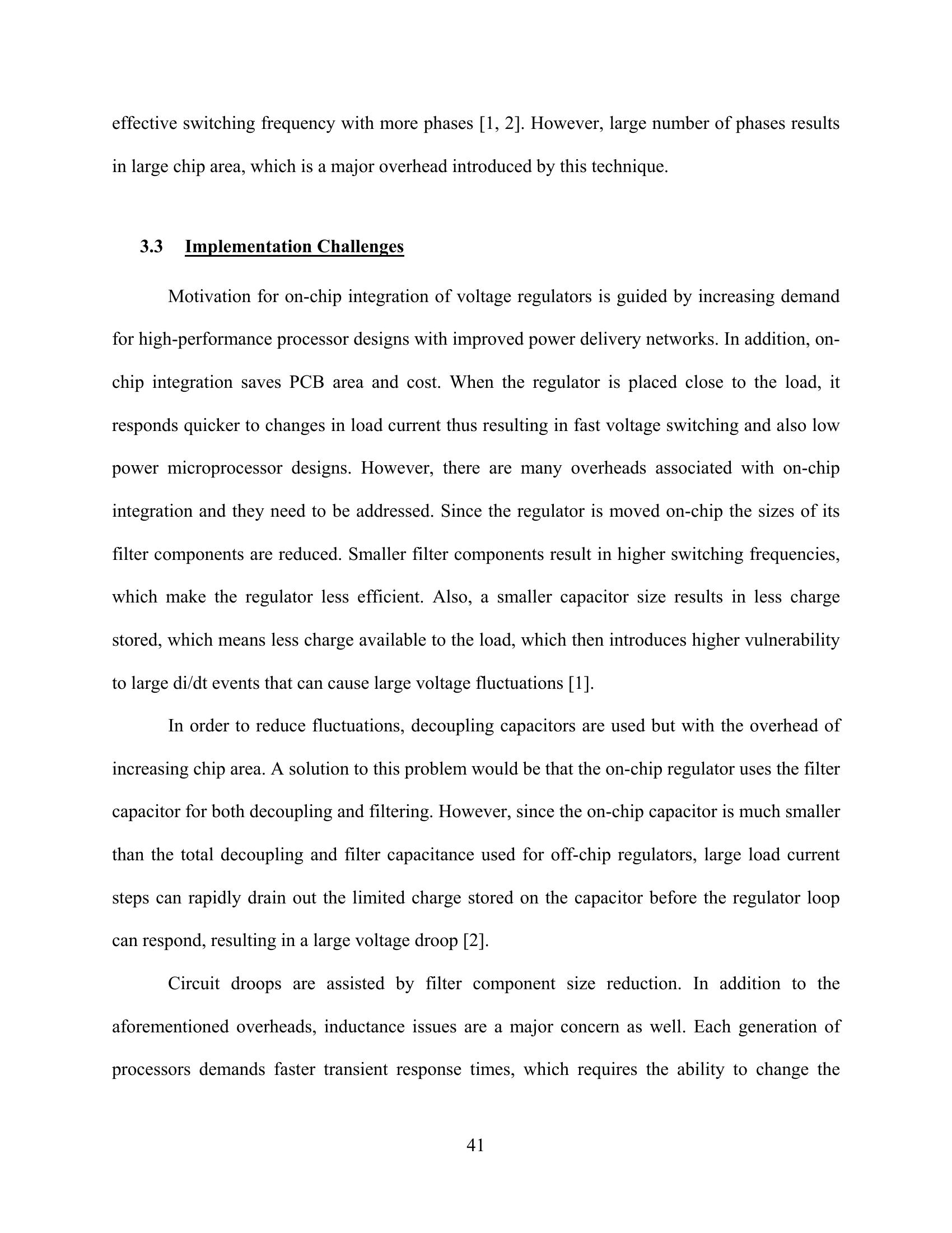
current through the inductor quickly. The magnetic field within an inductor resists change as in
(3-1). Since the regulator provides constant output voltage, the only way to increase di/dt is to
reduce the inductance value. A decrease in inductance size results not only in faster switching
and higher inductor ripple current, but in a more noticeable parasitic inductance in the circuit as
well.
di V
= OUT (3-1)
dt L
Although it remains a challenge to fabricate an on-chip inductor, it can still be realized in
today’s integrated circuit technology, but the low inductance values of on-chip inductors are only
suitable for RF applications [6]. Due to these limitations it becomes necessary to avoid
inductance when dealing with on-chip regulators. Potential candidates to replace an inductor are
gyrators, which consist of a capacitor, resistors, and transistors. An inductor realized with a
gyrator improves the quality of filter networks. Gyrator application reduces the size and cost of a
system by removing the need for bulky, heavy and expensive inductors.
Other inductorless methods include, conventional linear regulators, which suffer from
low efficiency, MEMS integrated inductors, which lack process compatibility with current
prevailing fabrication processes and high cost, and finally charge pumps, which suffer from
pulsating currents that eventually cause poor output voltage regulation. Therefore, the gyrator
replacement of inductor looks the most attractive technique. In this chapter we focus in reducing
the voltage droop in the circuit. Methods for replacing the inductor will be presented in our
future work.
42
3.4 Hot Swap Controller Solution
When the voltage regulator is implemented on-chip, the sizes of filter elements are
reduced due to high switching frequencies. As a result, the circuit becomes more vulnerable to
voltage droops and current surges. A smaller capacitor stores less charge and if the load is
experiencing a large current step it will quickly drain this small amount of charge stored, thus
resulting in output voltage droop. Also, switching power supplies experience inrush currents at
turn on due to switching elements, which is undesirable for the load. In order to eliminate these
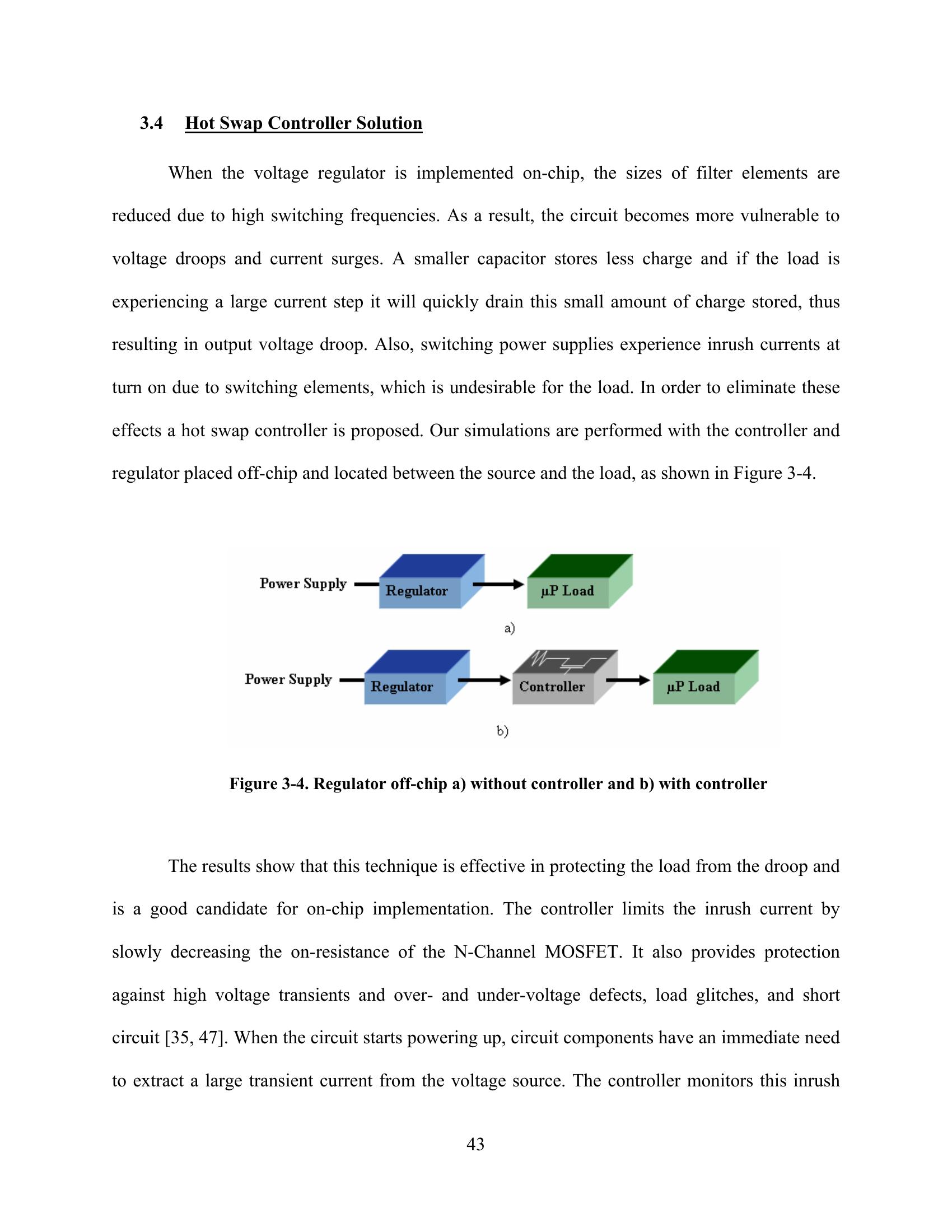
effects a hot swap controller is proposed. Our simulations are performed with the controller and
regulator placed off-chip and located between the source and the load, as shown in Figure 3-4.
Figure 3-4. Regulator off-chip a) without controller and b) with controller
The results show that this technique is effective in protecting the load from the droop and
is a good candidate for on-chip implementation. The controller limits the inrush current by
slowly decreasing the on-resistance of the N-Channel MOSFET. It also provides protection
against high voltage transients and over- and under-voltage defects, load glitches, and short
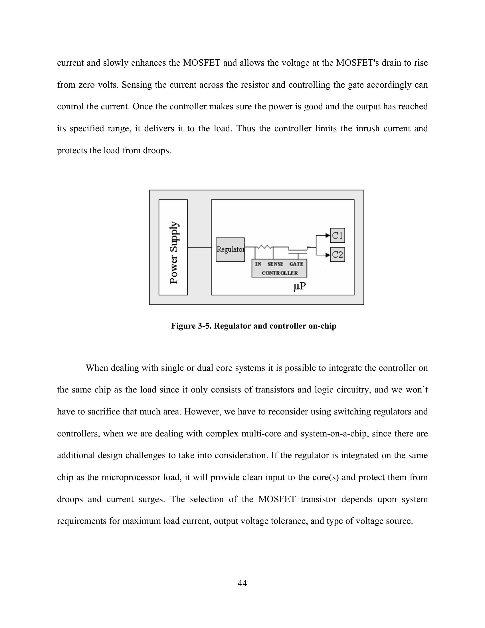
circuit [35, 47]. When the circuit starts powering up, circuit components have an immediate need
to extract a large transient current from the voltage source. The controller monitors this inrush
43
current and slowly enhances the MOSFET and allows the voltage at the MOSFET’s drain to rise
from zero volts. Sensing the current across the resistor and controlling the gate accordingly can
control the current. Once the controller makes sure the power is good and the output has reached
its specified range, it delivers it to the load. Thus the controller limits the inrush current and
protects the load from droops.
Figure 3-5. Regulator and controller on-chip
When dealing with single or dual core systems it is possible to integrate the controller on
the same chip as the load since it only consists of transistors and logic circuitry, and we won’t
have to sacrifice that much area. However, we have to reconsider using switching regulators and
controllers, when we are dealing with complex multi-core and system-on-a-chip, since there are
additional design challenges to take into consideration. If the regulator is integrated on the same
chip as the microprocessor load, it will provide clean input to the core(s) and protect them from
droops and current surges. The selection of the MOSFET transistor depends upon system
requirements for maximum load current, output voltage tolerance, and type of voltage source.
44
25
20
15
10
5
0
5.00 5.05 5.10 5.15 5.20 5.25 5.30 5.35 5.40 5.45 5.50
-5
-10
-15
-20
-25
Time(ms)
45
)A(tnerruC
I(Supply)
I(Load)
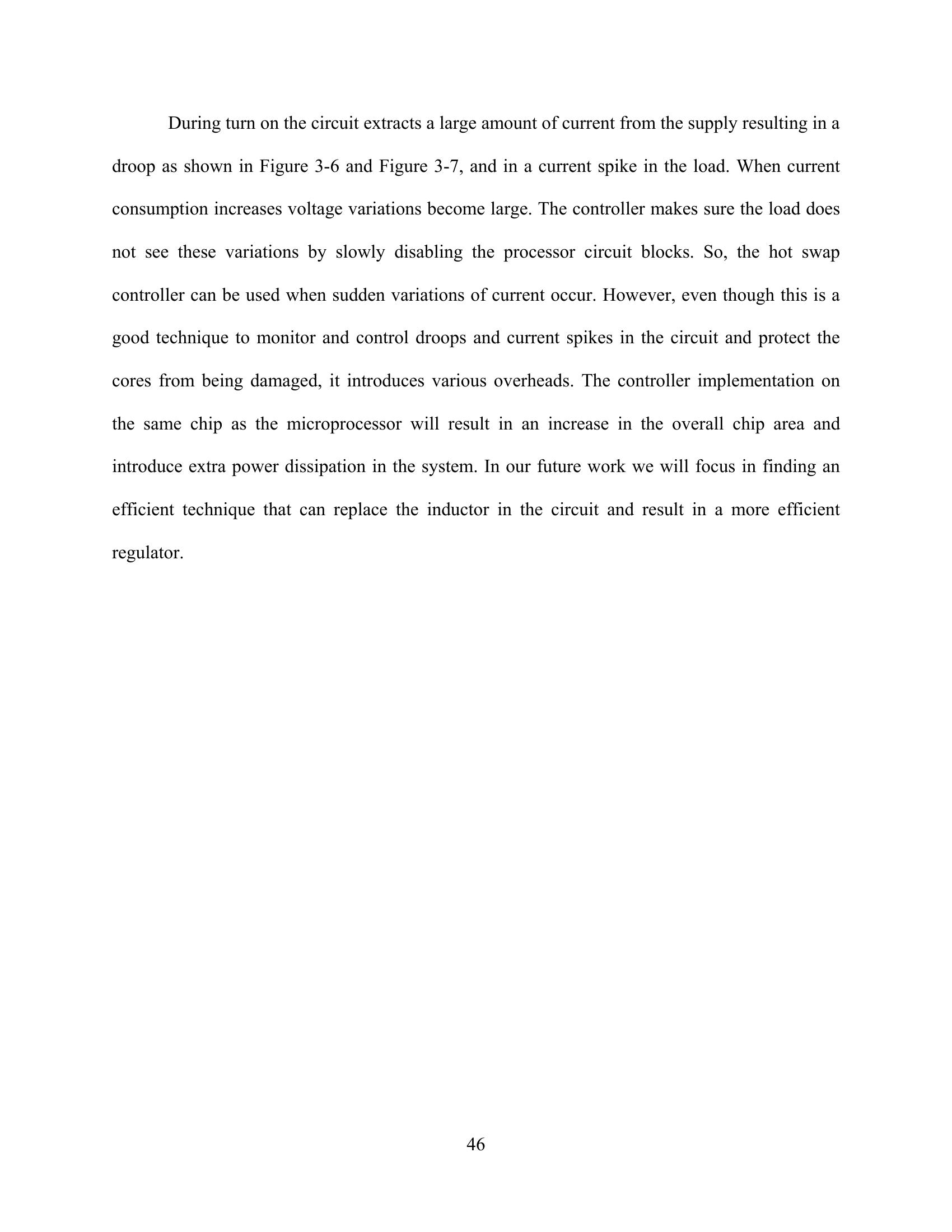
Figure 3-6. Inrush current effects in the supply and load
10
5
0
5.00 5.10 5.20 5.30 5.40 5.50
-5
-10
-15
-20
-25
Time(ms)
)A(tnerruC
I(Supply)
I(Load)
Figure 3-7. Inrush current protection
| I(S | ||||||||
| None | None | None | None | None | None | None | None | upply) |
| I(L | oad) | |||||||
| 00 5. | 05 5. | 10 5. | 15 5. | 20 5.2 | 5 5.30 | 5.35 | 5.40 5. | 45 5 |
| 0 5.1 | 0 5. | 20 5.30 | 5 | .40 5.5 |
| I(Supply) I(Load) |
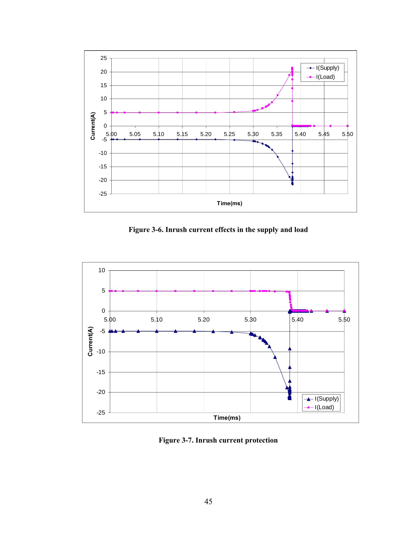
During turn on the circuit extracts a large amount of current from the supply resulting in a
droop as shown in Figure 3-6 and Figure 3-7, and in a current spike in the load. When current
consumption increases voltage variations become large. The controller makes sure the load does
not see these variations by slowly disabling the processor circuit blocks. So, the hot swap
controller can be used when sudden variations of current occur. However, even though this is a
good technique to monitor and control droops and current spikes in the circuit and protect the
cores from being damaged, it introduces various overheads. The controller implementation on
the same chip as the microprocessor will result in an increase in the overall chip area and
introduce extra power dissipation in the system. In our future work we will focus in finding an
efficient technique that can replace the inductor in the circuit and result in a more efficient
regulator.
46
4 TWO-STAGE APPROACH FOR VOLTAGE REGULATOR
IMPLEMENTATION IN SOC
Technology evolution [37] has resulted in system-on-a-chip, which is a promising
solution for integrating heterogeneous components such as digital signal processor (DSP) chips,
memory cores, sensors, encoder blocks, micro-electro-mechanical systems (MEMS), and
optoelectronic devices. Figure 4-1 shows a system-on-a-chip, which includes flash memory,
SDRAM memory, GPS block, I²C interface, and various other function blocks.
Figure 4-1. STA2052, System-on-chip, from Nikkei Electronics Asia
47
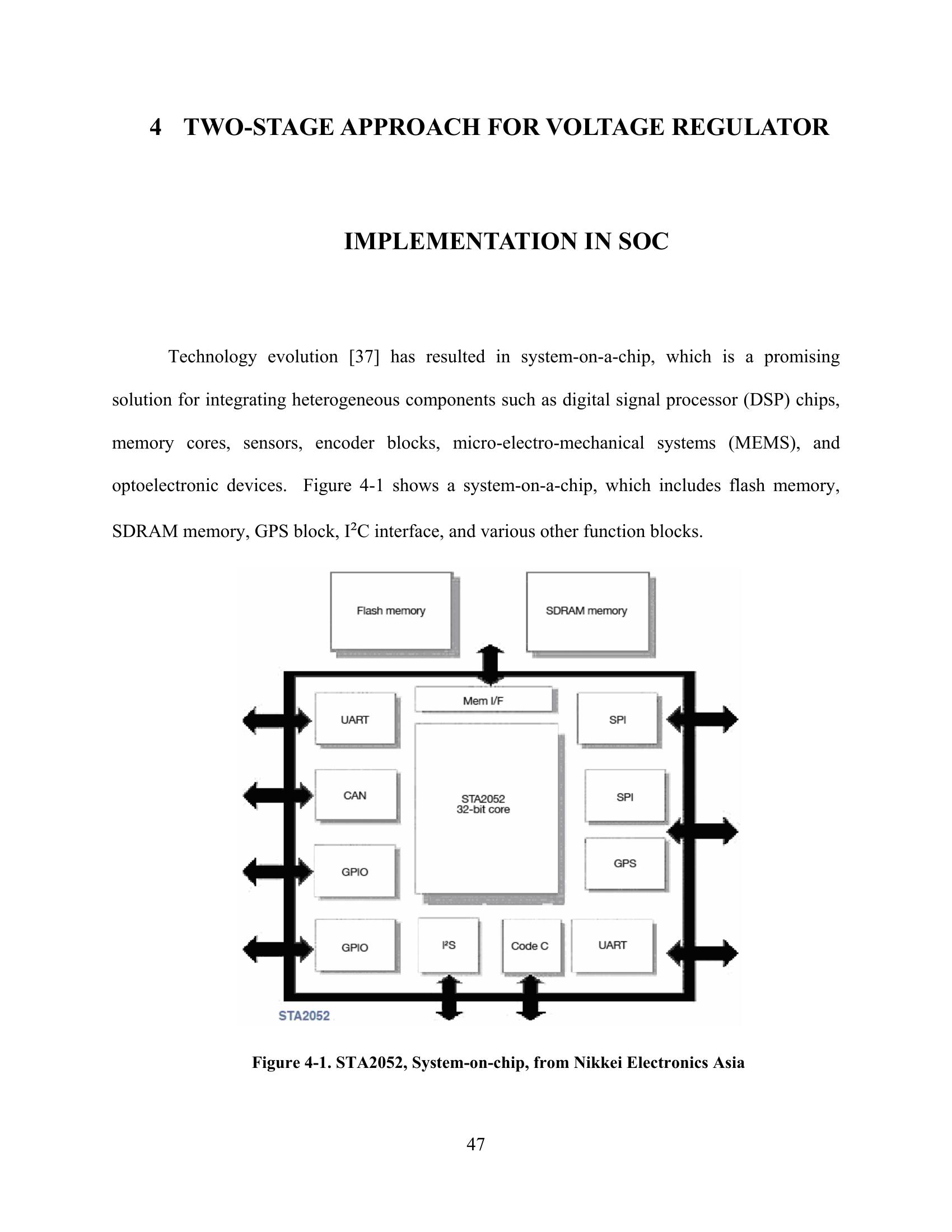
As Figure 4-1 reveals, SOC design includes highly integrated mixed-signal integrated
circuits, which are popular due to their low-cost, low power, and low-area [18]. Since analog and
digital parts are integrated on the same chip along with a large number of cores, there will be
issues related to management of power consumption and temperature, both of which directly
affect the SOC reliability [19]. Due to the increase in circuit density, analog and digital parts are
in close proximity, which causes signal noise. Therefore, voltage regulator becomes a crucial
component of the power management system. Voltage regulators provide constant voltage and
filter fluctuations that are generated from the power supply, thus protecting the load from seeing
the ripple that comes from the input.
The regulator needs to be designed according to function block specifications and provide
good efficiency and transient response characteristics. The voltage regulator typically resides
between the source and each load. Since an SOC includes the integration of various function
blocks, multiple voltage domains are needed. Multiple supply voltages provide an effective
technique for power optimization [24], which results in better performance, low power
dissipation, and evenly distributed heat dissipation. This strategy has also the advantage of
allowing modules along the critical paths to operate with the highest available voltage level,
while permitting modules along non-critical paths to use a lower voltage [26], thus decreasing
energy consumption.
48
4.1 Hybrid Two-Stage Regulator
Users of portable electronic devices and embedded systems have placed increasing
demands on the industry to create devices with high performance that have the ability to handle
more complex tasks. In addition to higher computational capabilities, low-power operation is
equally, if not more important [1]. The solution of [17] includes a combination of a variety of
voltage regulators such as switching, linear, and switched capacitor regulators, not only for
power management but for system protection against power analysis attacks as well. However,
the design of such devices is not an easy task to accomplish and it occupies significant area.
Aggressive power management is required and especially an efficient voltage regulator that not
only provides well-regulated voltage to the system but also keeps its cost low. Since the regulator
resides between the source and the load it provides power to, its design experiences challenges
coming from both the input side and the load side. The challenge coming from the input side
includes an input voltage that is higher than the operating voltage of the chip and the challenge
coming from the load side includes severe transient.
Supply
DRAM @1.5V,
Switching LDO0
30mA
Regulator
DSP @1.2V,
LDO1 70mA
Sensor @1.0V,
LDO2 4mA
Figure 4-2. Two-stage conversion
49
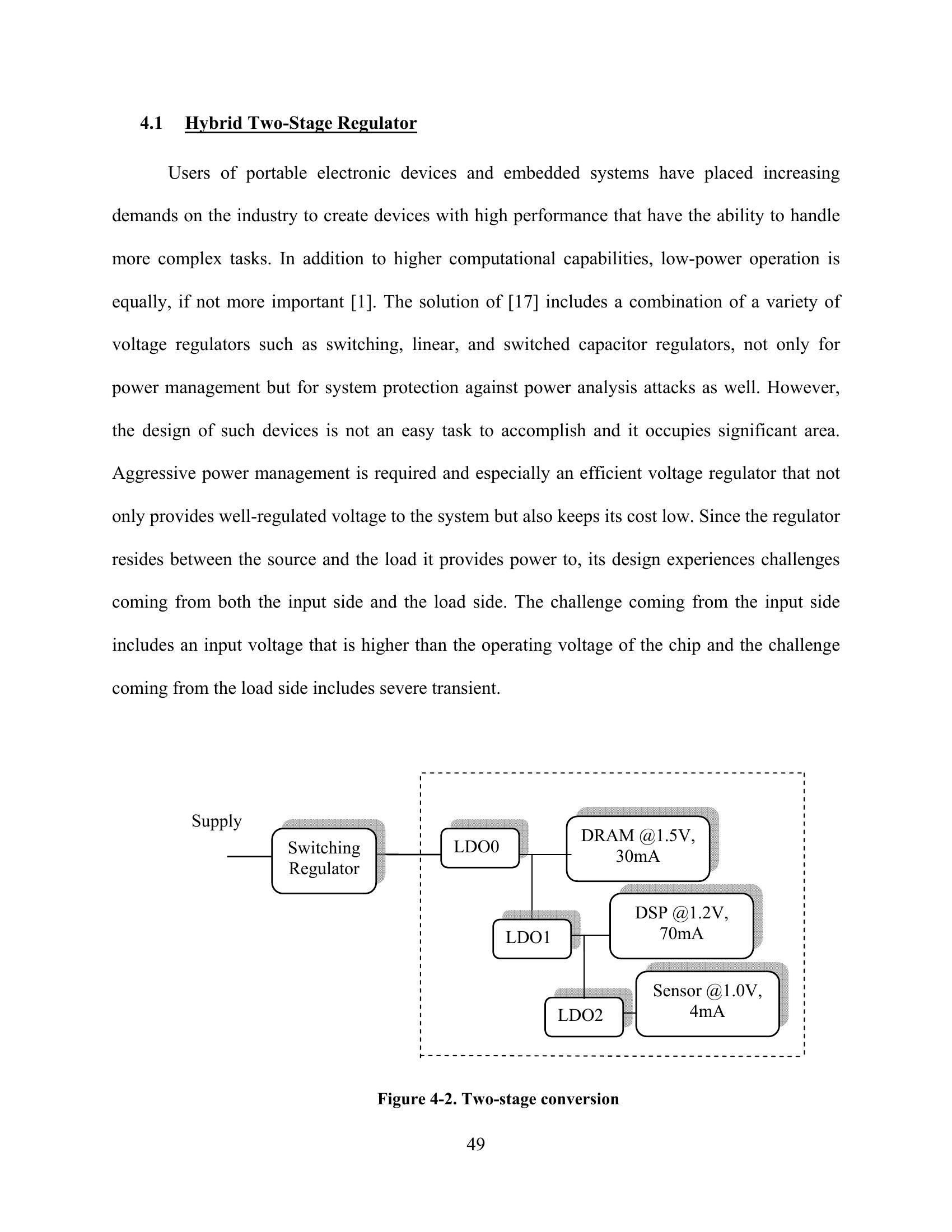
Furthermore, since the load is a system-on-a-chip employing many functional blocks it is
very difficult for the single-stage converter to handle challenges from both sides. In other words,
we need a two-stage conversion where the first stage steps down the voltage from the power
supply and the second stage steps it down to bring it close to the level required by the load. If
both of these regulator stages are placed off-chip it would not improve the transient response due
to interconnect parasitic components that would still fall between the regulator and the load. On
the other hand, due to their large size, complexity, and cost it is not practical to place switching
regulators on the same chip as the load. Therefore, the first stage, a switching regulator, will be
placed off-chip and the second stage, a tree design of low dropout linear regulators, will be
placed on the same chip as the load. This improves the transient response of the regulator and it
also reduces the noise produced by the switching regulator.
Buck-type switching regulator is used as first stage since it is needed to step down the
battery voltage to a lower level as required by the SOC. In addition, the efficiency of switching
regulators is generally higher than efficiency of linear regulators due to the presence of the
inductor as low loss device. In this design a high efficiency first stage is needed since it will
provide power to the second stage therefore the switching regulator is placed off-chip. The buck
converter generates the 1.8V bus at a higher efficiency than the LDO. Low dropout linear
regulators are used as the second stage and placed on-chip due to their small size, low cost,
simplicity, and the ability to reduce fluctuations coming from the power source. The switching
regulator – LDO solution uses a buck converter to generate the 1.8V rail, and an LDO powered
from 1.8V to generate the 1.5V output. Then the 1.5V output will feed a DRAM chip and it will
also serve as input to second LDO. Second LDO will step down the voltage to 1.2V to feed a
DSP chip as specified in [34]. This 1.2V output will serve as input to third LDO, which will step
50
down the voltage to 1.0V and feed a sensor. This solution is a good overall compromise between
size, cost, heat dissipation, and efficiency.
4.2 Stage 1: Switching Regulator
The first stage of this approach employs a switching regulator to step down the battery
voltage and serve as power source for the second stage.
Figure 4-3. Switching regulator
The switching regulator, shown in Figure 4-3, uses a PMOS transistor as a switch that
connects and disconnects the input voltage to the external inductor, which is connected to the
output terminal. Inductor current is equal to the output current. When the switch is in the ON
position, shown in Figure 4-4, the input voltage is connected to the inductor, which causes a
voltage difference to appear across the inductor, and thus an increase in the current through it [4].
This current will flow through the inductor and charge the capacitor.
Alternatively, when the switch is in the OFF position, Figure 4-5, the input voltage
applied to the inductor is removed. However, since the inductor current does not change
instantly, the voltage across it will adjust to hold the current constant. The decreasing current
causes the input end of the inductor to have a negative voltage. This turns on the diode, and the
51
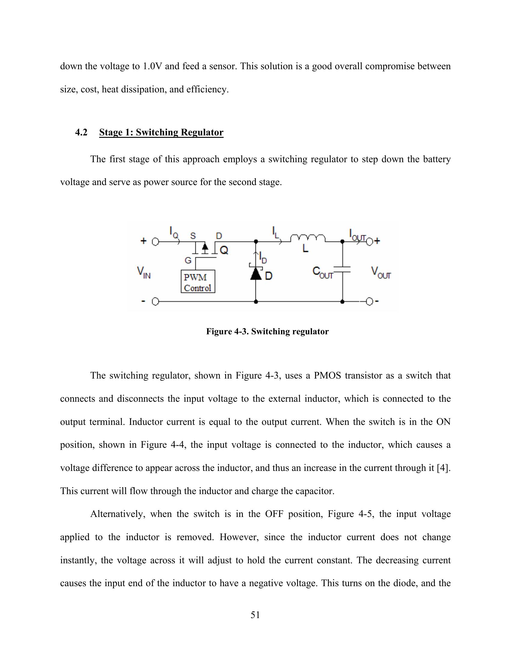
inductor current flows through the load and back through the diode. During the OFF state, the
capacitor discharges into the load and contributes to the total current being supplied to the load.
The output of the LC low-pass filter, V , is the output voltage of the regulator that powers the
OUT
load. The filter attenuates the high frequency square wave and therefore V experiences ripple
OUT
[1, 2]. The intrinsic switched nature of these regulators not only produces ripples but also an
increment of electromagnetic interference in neighboring electronic systems [22]. Figure 4-4 and
Figure 4-5 show current flow in the switching regulator when the switch is closed and when it is
open.
Figure 4-4. Switching regulator with switch ON
Figure 4-5. Switching regulator with switch OFF
Current and voltage waveforms during switching are shown in figures below.
52
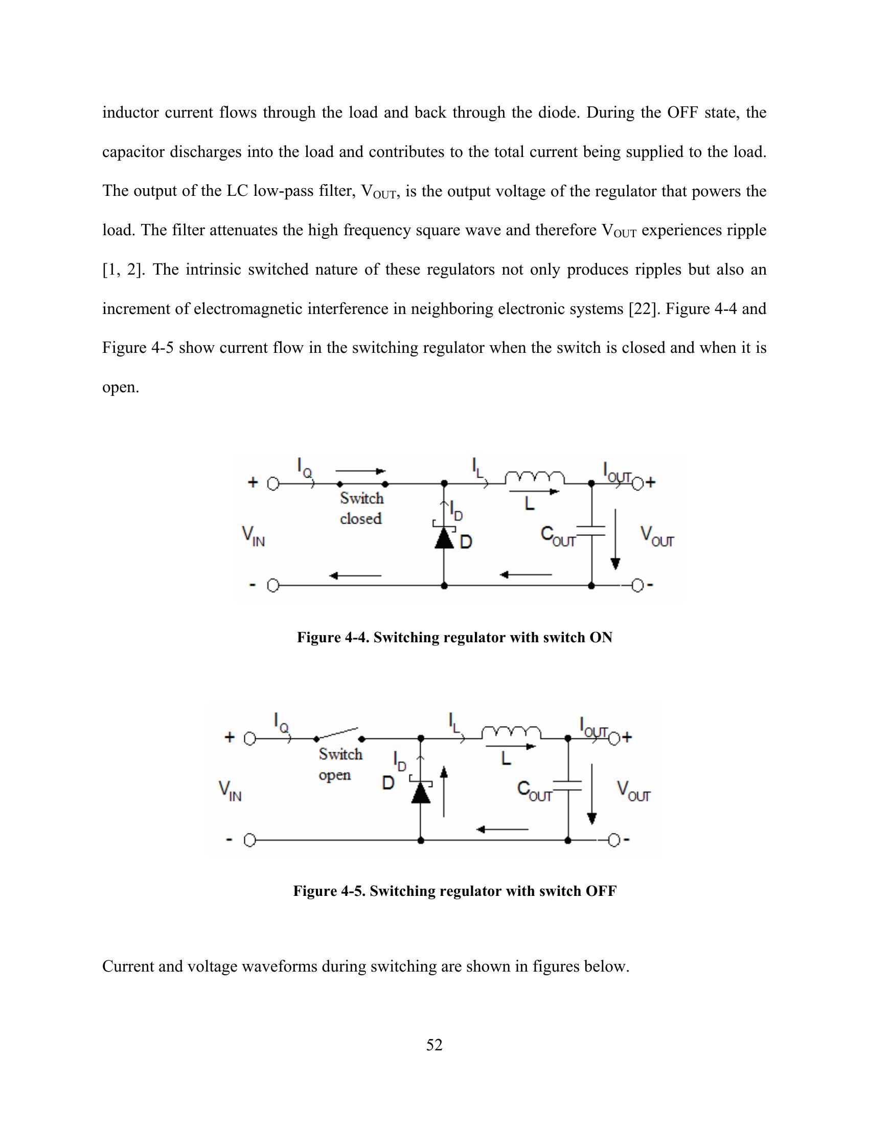
Figure 4-6. PWM, duty cycle of the switching regulator
Figure 4-7. Voltage drain-source ,V , waveform
DS
Figure 4-8. Waveform of current through PMOS transistor
Figure 4-9. Waveform of current through diode
53
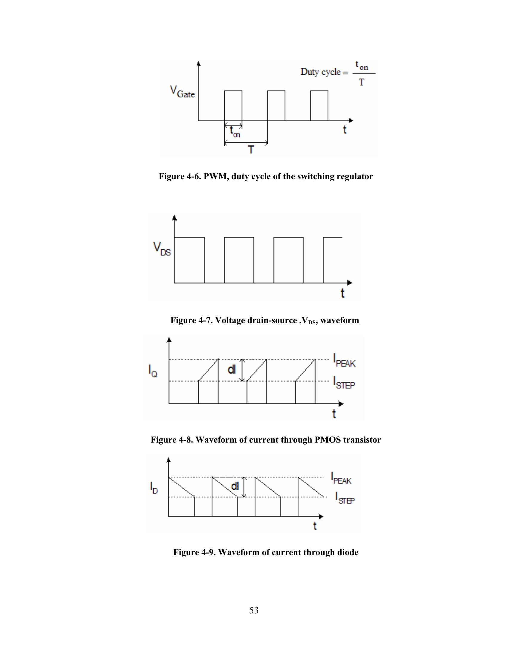
Figure 4-10. Current through inductor/output current
The rectifier used for the design of the switching regulator is a Schottky diode because it
provides low forward voltage and good reverse recovery characteristics. The output capacitor is
used in order to provide significant filtering of the switching ripple. The selected capacitor is
large enough so that its impedance is much smaller than the load at the switching frequency,
allowing most of the ripple current to flow through the capacitor and not the load. The ripple
current flowing through the output capacitor is equal to the inductor current waveform.
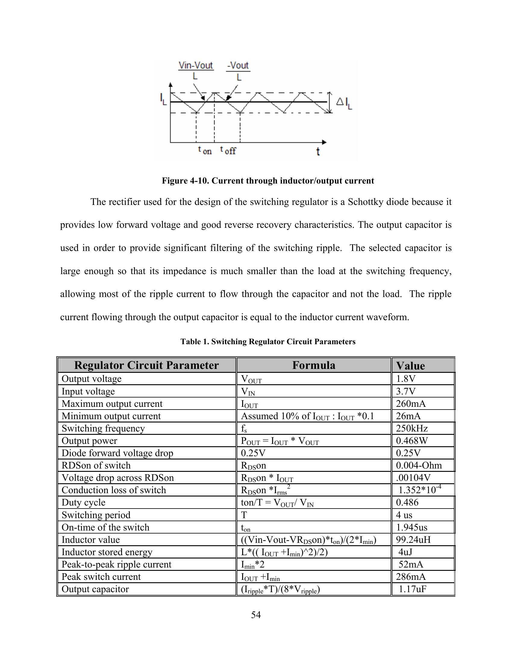
Table 1. Switching Regulator Circuit Parameters
Regulator Circuit Parameter Formula Value
Output voltage V 1.8V
OUT
Input voltage V 3.7V
IN
Maximum output current I 260mA
OUT
Minimum output current Assumed 10% of I : I *0.1 26mA
OUT OUT
Switching frequency f 250kHz
s
Output power P = I * V 0.468W
OUT OUT OUT
Diode forward voltage drop 0.25V 0.25V
RDSon of switch R on 0.004-Ohm
DS
Voltage drop across RDSon R on * I .00104V
DS OUT
Conduction loss of switch R on *I 2 1.352*10-4
DS rms
Duty cycle ton/T = V / V 0.486
OUT IN
Switching period T 4 us
On-time of the switch t 1.945us
on
Inductor value ((Vin-Vout-VR on)*t )/(2*I ) 99.24uH
DS on min
Inductor stored energy L*(( I +I )^2)/2) 4uJ
OUT min
Peak-to-peak ripple current I *2 52mA
min
Peak switch current I +I 286mA
OUT min
Output capacitor (I *T)/(8*V ) 1.17uF
ripple ripple
54
| Regulator Circuit Parameter | Formula | Value | ||||||
| Output voltage | None | None | V OUT | None | None | 1.8V | None | None |
| Input voltage | None | None | V IN | None | None | 3.7V | None | None |
| Maximum output current | None | None | I OUT | None | None | 260mA | None | None |
| Minimum output current | None | None | Assumed 10% of I : I *0.1 OUT OUT | None | None | 26mA | None | None |
| Switching frequency | None | None | f s | None | None | 250kHz | None | None |
| Output power | None | None | P = I * V OUT OUT OUT | None | None | 0.468W | None | None |
| Diode forward voltage drop | None | None | 0.25V | None | None | 0.25V | None | None |
| RDSon of switch | None | None | R on DS | None | None | 0.004-Ohm | None | None |
| Voltage drop across RDSon | None | None | R on * I DS OUT | None | None | .00104V | None | None |
| Conduction loss of switch | None | None | R on *I 2 DS rms | None | None | 1.352*10-4 | None | None |
| Duty cycle | None | None | ton/T = V / V OUT IN | None | None | 0.486 | None | None |
| Switching period | None | None | T | None | None | 4 us | None | None |
| On-time of the switch | None | None | t on | None | None | 1.945us | None | None |
| Inductor value | None | None | ((Vin-Vout-VR on)*t )/(2*I ) DS on min | None | None | 99.24uH | None | None |
| Inductor stored energy | None | None | L*(( I +I )^2)/2) OUT min | None | None | 4uJ | None | None |
| Peak-to-peak ripple current | None | None | I *2 min | None | None | 52mA | None | None |
| Peak switch current | None | None | I +I OUT min | None | None | 286mA | None | None |
| Output capacitor | None | None | (I *T)/(8*V ) ripple ripple | None | None | 1.17uF | None | None |
4.2.1 Pulse Width Modulation (PWM)
The duty cycle of the switching regulator is modulated by pulse width modulation in
order to control the amount of power sent to the load. It measures the output voltage and when it
is lower than the desired voltage of 3.7V it turns on the switch. When output voltage increases
above 3.7V, PWM turns off the switch. The desired output voltage is realized by switching
voltage to the load with the appropriate duty cycle. Since V is 3.7V and V is 1.8V then duty
IN OUT
cycle is 1.8V/3.7V=0.486. The step-down occurring is relatively small, from 3.7V to 1.8V,
therefore the operating duty cycle of the regulator is sufficient to maintain high regulator
efficiency. On the other hand, if the step-down was bigger, such as from 10V to 1.8V, then duty
cycle would be 1.8V/10V= .180, which is very small and makes it difficult to design a voltage
regulator with high efficiency. In addition, duty cycle is also dependent on t which is 1.94us,
on,
and period, T, which is 4us. So, efficiency of the regulator varies with duty cycle. An extreme
duty cycle challenges the design of an efficient regulator.
4.2.2 Switching Regulator Efficiency
Efficiency is one of the most important features of the switching regulator. The first stage
of the design needs to be very efficient since it will step down the battery voltage and also serve
as source for the on-chip LDO branches. The switching regulator provides high efficiency, given
by (4-1), because it employs an inductor that transfers energy from input to output in a lossless
manner.
P V * I
η= LOAD = OUT LOAD (4-1)
P V * I
TOTAL IN IN(AVE)
55
Furthermore, the switch mode transistor in the circuit also provides minimum loss since ideally
its power dissipation is zero. When the switch is closed there will be zero voltage and therefore
zero power dissipation and when the switch is open there will be zero current and zero power
dissipation. The efficiency of the switching regulator depends on the size of its filter
components, inductor and capacitor. The size of the inductor determines the shape of the output
ripple current and voltage.
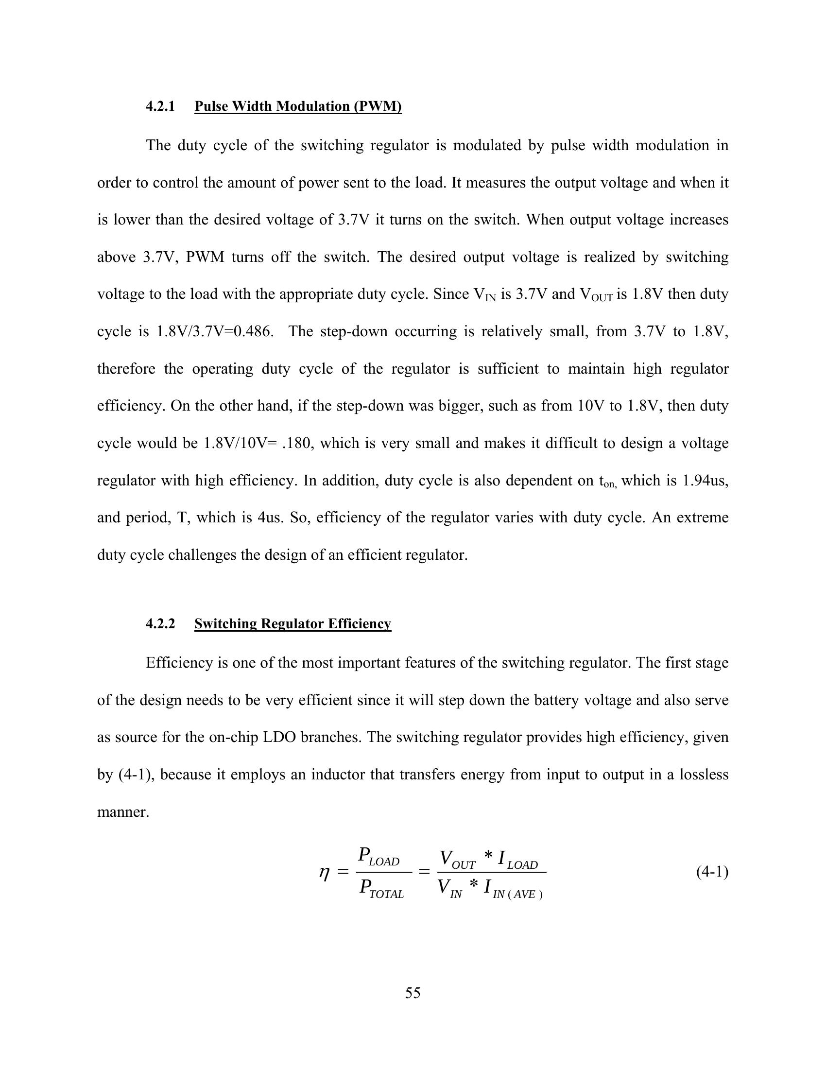
As seen in equation (4-2), mathematically, in order to reduce output ripple current and
voltage, the size of the inductor has to be large, and this is one of the reasons why the switching
regulators are not a good choice for SOC solutions. The large size of the inductor prohibits its
SOC implementation.
V −V
IN OUT
∆I = *t (4-2)
L
L
on
Figure 4-11, shows the impact that inductor sizing has on output voltage ripple.
Voltage Ripple vs. Inductance
600
500
400
300
200
100
0
0 10 20 30 40 50 60 70
Inductance (uH)
56
)Vm(
elppirV
Figure 4-11. Voltage ripple dependency on inductor size
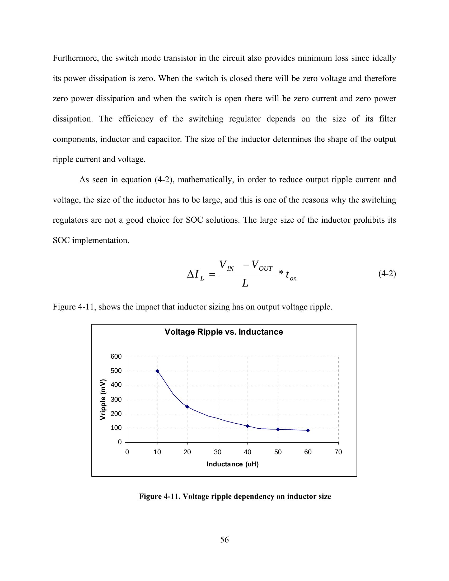
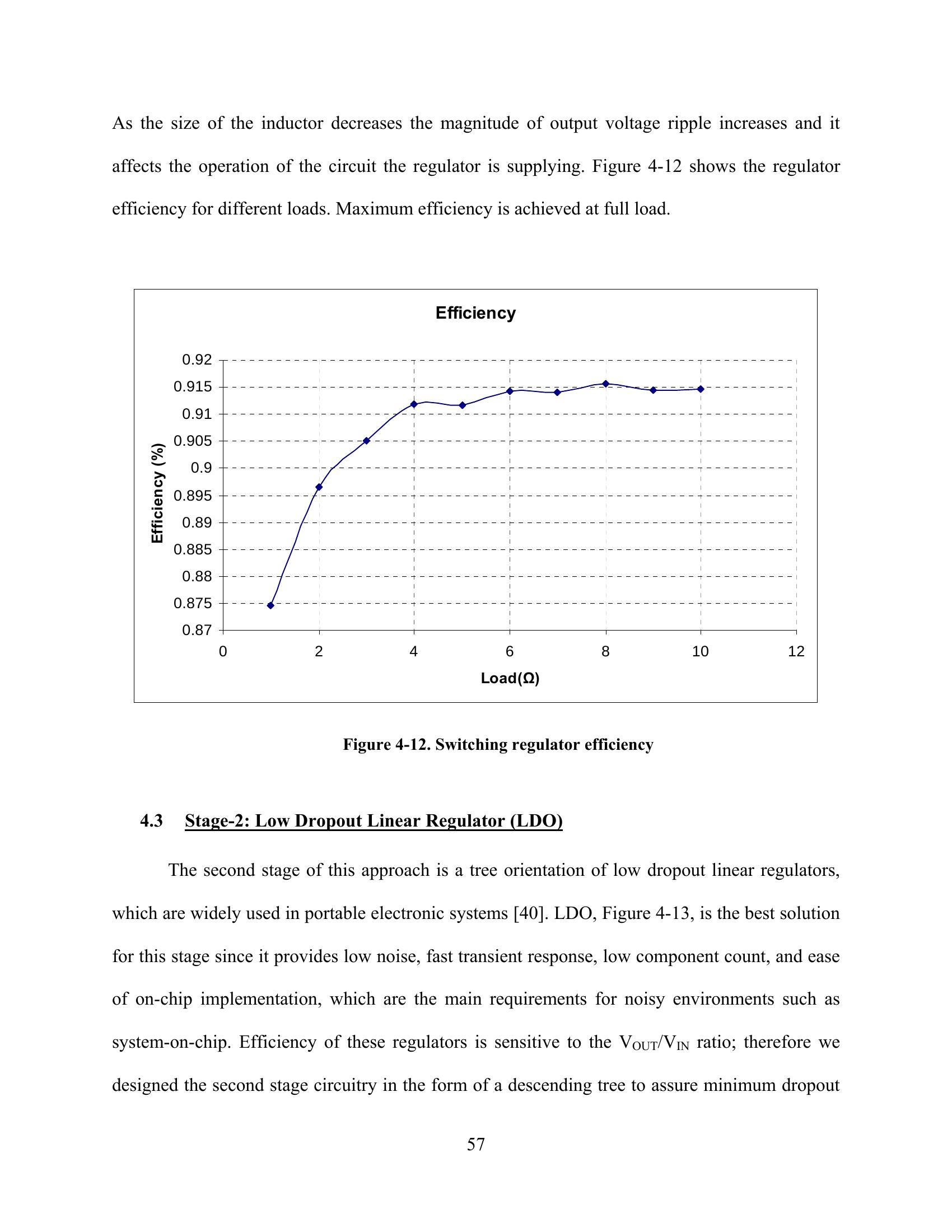
As the size of the inductor decreases the magnitude of output voltage ripple increases and it
affects the operation of the circuit the regulator is supplying. Figure 4-12 shows the regulator
efficiency for different loads. Maximum efficiency is achieved at full load.
Efficiency
0.92
0.915
0.91
0.905
0.9
0.895
0.89
0.885
0.88
0.875
0.87
0 2 4 6 8 10 12
Load(Ω)
57
)%(
ycneiciffE
Figure 4-12. Switching regulator efficiency
4.3 Stage-2: Low Dropout Linear Regulator (LDO)
The second stage of this approach is a tree orientation of low dropout linear regulators,
which are widely used in portable electronic systems [40]. LDO, Figure 4-13, is the best solution
for this stage since it provides low noise, fast transient response, low component count, and ease
of on-chip implementation, which are the main requirements for noisy environments such as
system-on-chip. Efficiency of these regulators is sensitive to the V /V ratio; therefore we
OUT IN
designed the second stage circuitry in the form of a descending tree to assure minimum dropout
across the regulator, as shown in Figure 4-2. When the dropout is small the regulator can be used
with reasonable conversion efficiency [20]. In this stage, minimum dropout is not only important
to achieve good conversion efficiency but also to minimize heat dissipation. If a system is prone
to heat dissipation, additional cooling systems will be required, which increases system cost. Due
to their small size, the LDOs allow us to create multiple supply voltages, which also assist in an
even distribution of heat across the chip. The LDO requires only an input and output capacitor.
This solution is the most economical.
Pass element Vout
Error amplifier
R1 IIload
R2
Vref
Figure 4-13. Linear dropout regulator
4.3.1 Pass Element
Out of various pass elements that could be selected such as BJT or n-channel MOSFET
(NMOS), the p-channel MOSFET (PMOS) was selected due to its low drain-source resistance,
its ability to provide low dropout voltage, and its gate driving requirements. N-channel devices
are usually used in designs where low dropout is not the primary concern. If the NMOS acts as
58
| Error amplifier | None |
| None |
| IIlo | ad |
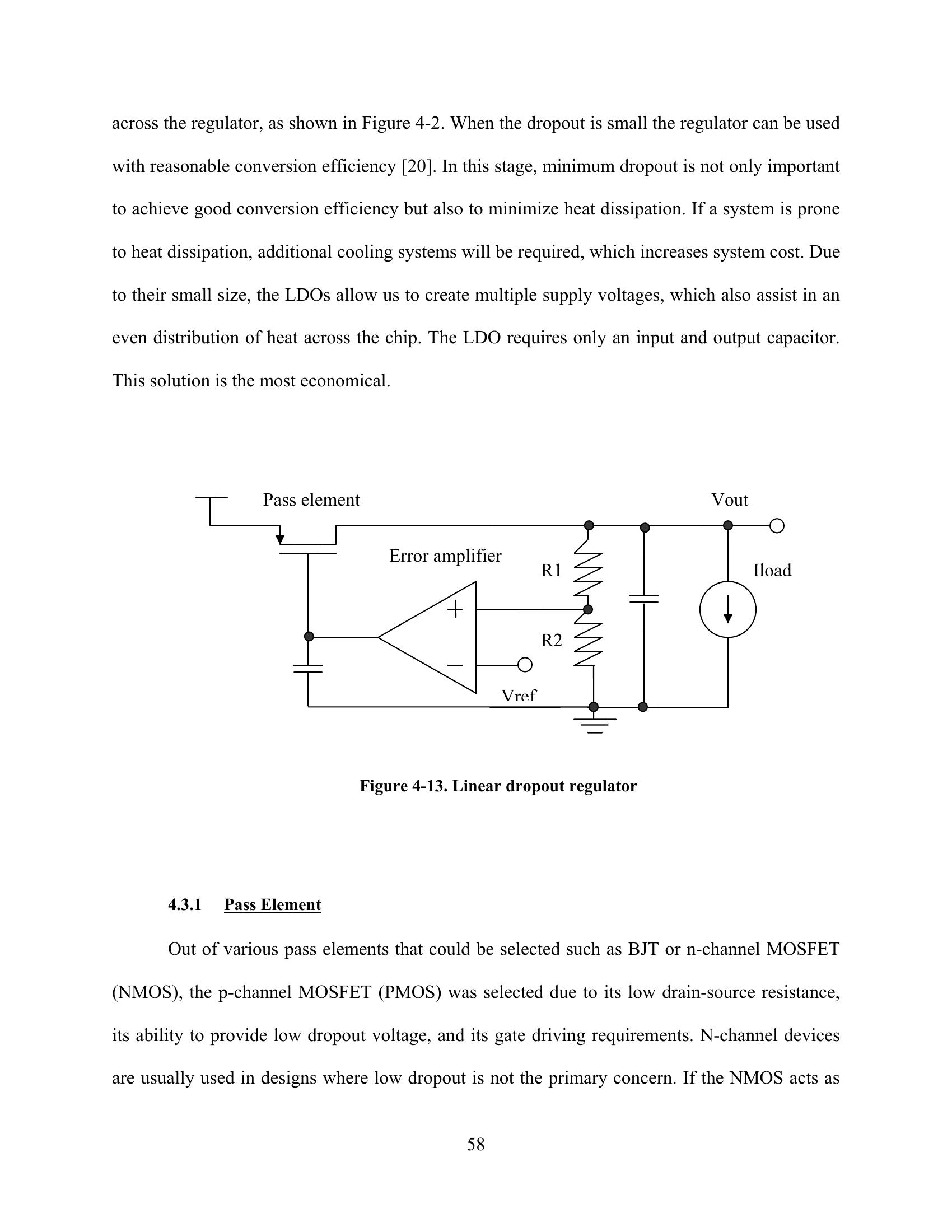
source follower, it will conduct the ripple from the gate to the output, and to keep the ripple low
we need to design a good error amplifier. On the other hand, the PMOS element that we have
selected acts like an adjustable resistor that allows high current flow when the gate becomes
more negative than the source and thus the drain-source resistance (R ) becomes small.
DS-on
Smaller the resistance, more current flows and therefore higher current efficiency is achieved.
Low power loss across the device is also obtained due to the PMOS low forward drop.
Pass element operates in the linear region in order to drop the input voltage to the desired
output voltage [45]. In the linear region, the transistor is turned ON and is able to conduct current
through the channel that has been created. Therefore, current flows from drain to source. The
conditions that need to be satisfied for the pass element to operate in the linear region are given
by (4-3) and (4-4).
V > V (4-3)
GS TH
V < (V – V ) (4-4)
DS GS TH
Here, V is the gate-source voltage, V is the drain-source voltage, and V is threshold
GS DS TH
voltage. The MOSFET operates like a resistor, controlled by the gate voltage relative to both the
source and drain voltages. Equivalent resistance of the transistor can be found since we know the
input voltage, output voltage, and load current. So, it is perfectly correct to remove the transistor
and replace it with its equivalent resistance, with the only drawback being lack of control. While
we can control and adjust the gate of the transistor according to circuit specifications, it is
impossible to do so with the resistor. Therefore, we conclude that the pass device is the most
59
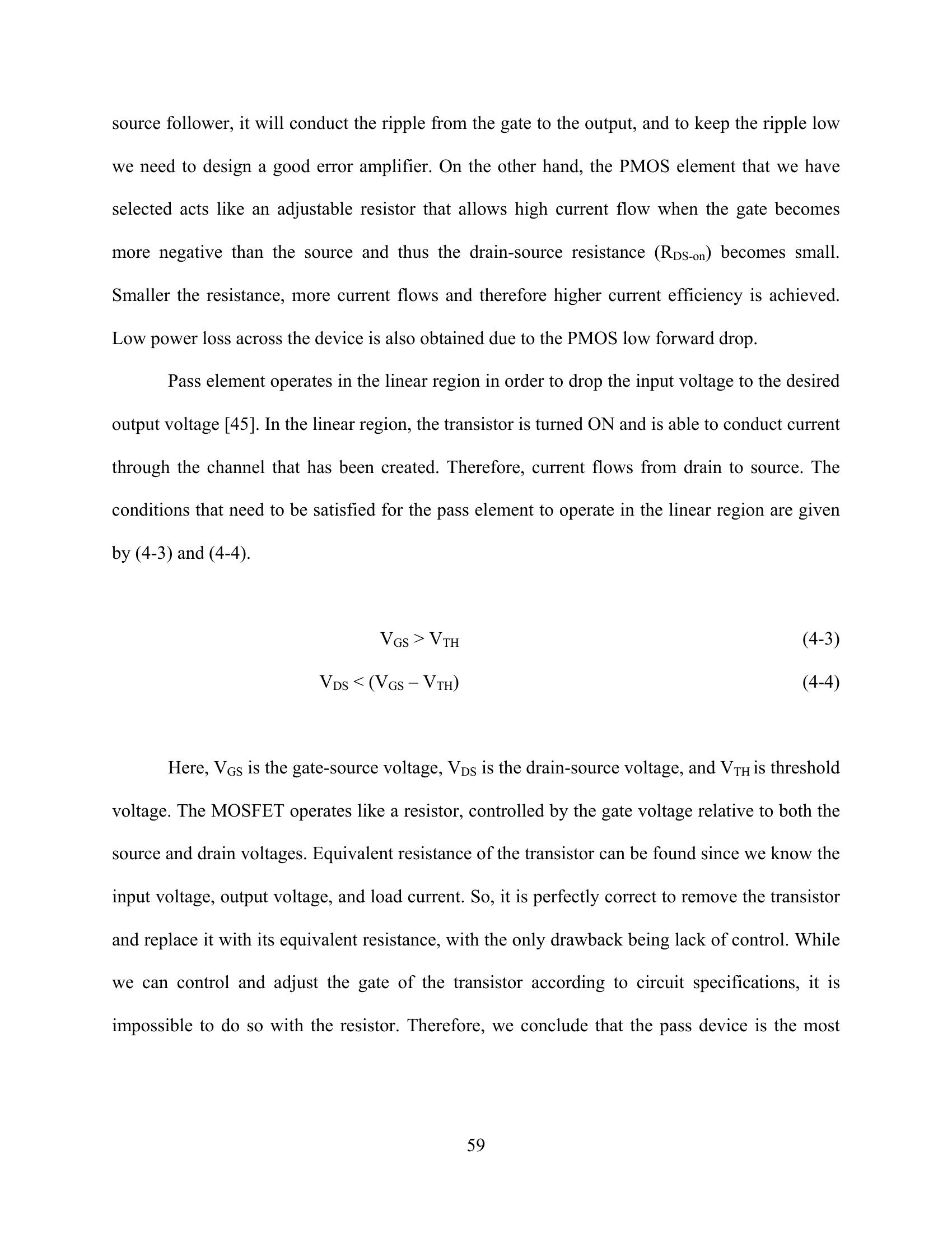
imperative and practical solution. In order to calculate the equivalent resistances of our three
pass devices, we use equation (4-5).
(V −V )
R = IN OUT (4-5)
eq I
LOAD
Using (4-5), for Branch-1, VIN is 1.8V, VOUT is 1.5V, and ILOAD is 30mA, and as a result
equivalent resistance is 1-Ohm. For Branch-2, VIN is 1.5V, VOUT is 1.2V, and ILOAD is
70mA, and as a result equivalent resistance is 0.4-Ohm. Finally, for Branch-3, VIN is 1.2V,
VOUT is 1.0V, and ILOAD is 4mA, and as a result equivalent resistance is 5-Ohm. The current-
voltage characteristics of the pass element are shown in Figure 4-14.
Figure 4-14. Current-Voltage characteristics [51]
60
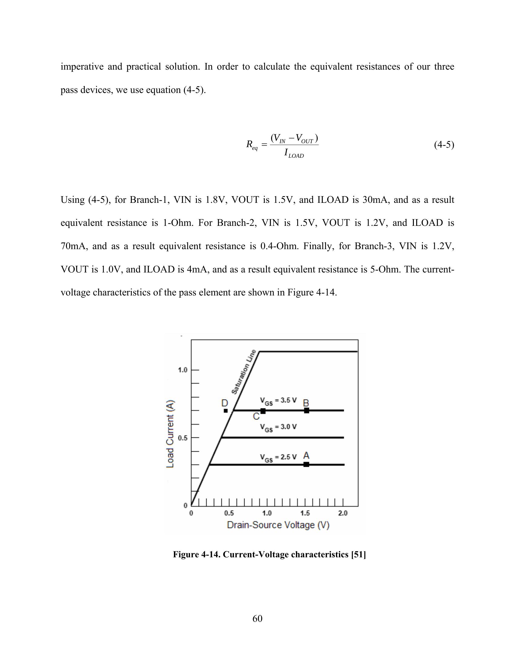
The drain to source voltage of the pass element is 1.5V with 30mA current, represented
by point A in Figure 4-14. At this operating point, point A, the voltage from gate to source will
be selected as 2.5V in order to maintain regulation. However, if a change occurs in the output
voltage, the LDO must react quickly in order to keep low dropout and low power dissipation. If
the load consumes more current, say 70mA, then the gate to source voltage will be increased by
the error amplifier to maintain regulation. This is represented by point B. So, a change in current
will result in a change in gate to source voltage but a change in drain to source voltage only
shifts the point accordingly as point C in the graph. However, from this point any further change
in voltage or current will bring the operating point in the saturation line. The saturation line is the
minimum MOSFET drain to source resistance (R ) [52]. If the LDO operates at point D,
DS-on
which is outside of the operating region, the LDO cannot reduce the drain to source voltage and
the output voltage falls out of regulation and transistor operates along the saturation line.
4.3.2 Error Amplifier
The error amplifier is a very important part of the LDO design. It senses changes in
output voltage and if V changes relative to V , which means if it exceeds regulation level,
OUT ref
the error amplifier decreases the differential voltage between gate-source allowing less current to
flow through PMOS thus decreasing V . On the other hand, if V decreases, the error
OUT OUT
amplifier increases the differential voltage between gate-source allowing more current to flow
through PMOS thus increasing V . The error amplifier used in this design is from Linear
OUT
Technology, LTC1469. The CMOS configuration of a Class-A error amplifier [41] is shown in
Figure 4-15. This type of amplifier is preferred in this LDO design since the low dropout
characteristics demand a PMOS output stage such as the one in the Class-A amplifier.
61
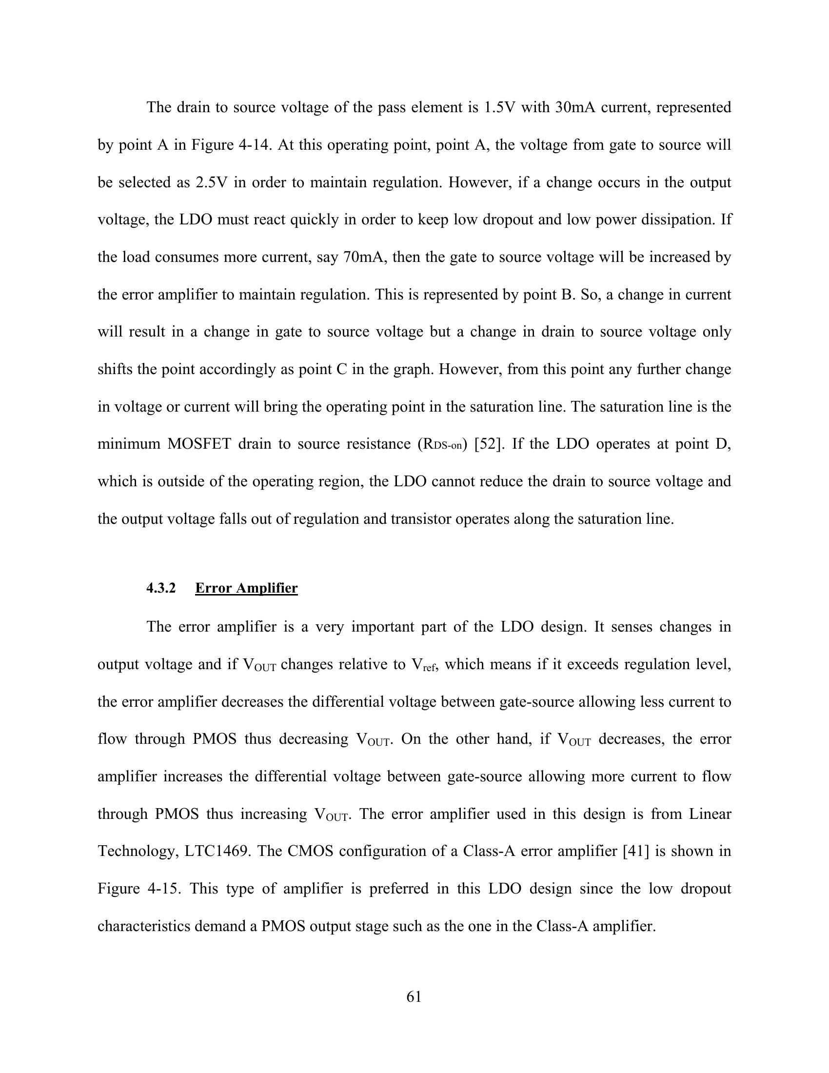
Figure 4-15. Class-A amplifier
Resistors R1 and R2 are bias resistors that form a voltage divider feedback network. In
order to get low quiescent current (ground current) consumption the values of these resistors
need to be large. Output capacitor value in the pico-range is selected such that it complies with
fabrication requirements.
4.3.3 Power Supply Ripple Rejection
Power supply ripple rejection (PSRR) is an important feature of the low dropout linear
regulator. It is the ability to prevent fluctuations at the output voltage caused by variations in the
input voltage [52]. It compares input and output ripple over a wide frequency range such as from
10Hz to 10MHz and it is measured in decibels (dB). [45] states that the specific formula to find
the PSRR for an LDO is given by:
62
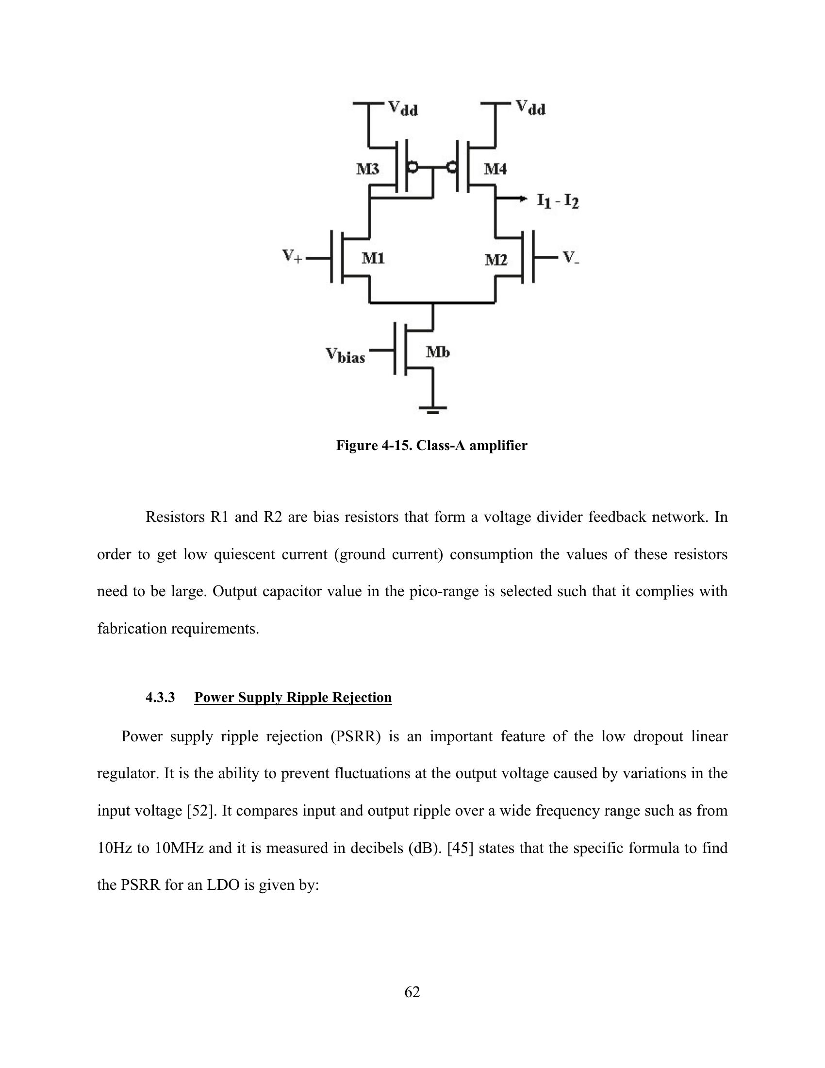
A Ripple
PSRR = 20log V = 20log IN (4-6)
A Ripple
VO OUT
Here, A is the feedback open-loop gain, and A is the gain from V to V with the
V VO IN OUT
feedback gain. In order to get high PSRR, A should be increased and A should be decreased.
V VO
Power supply ripple rejection at 250 kHz frequency is measured by modulating the input voltage
and measuring the change on the output.
4.3.4 Efficiency of Low Dropout Linear Regulator
Current efficiency and regulator efficiency are crucial in any regulator design, especially
when designing linear regulator since their efficiency is dependent on V /V ratio. Current
OUT IN
efficiency is especially important since it directly affects battery life. When the circuit is
operating at full load conditions, load current is much higher than quiescent current, however,
when the circuit is operating at low load conditions, quiescent current plays a dominant role.
Efficiency of the low dropout regulator is given by equation (4-7) and current efficiency is given
by equation (4-8).
V ∗I
η= OUT OUT (4-7)
(I + I )∗V
OUT quesc IN
I
η = OUT (4-8)
current (I + I )
OUT quesc
Corresponding efficiencies were calculated using equations (4-7) and (4-8).
63
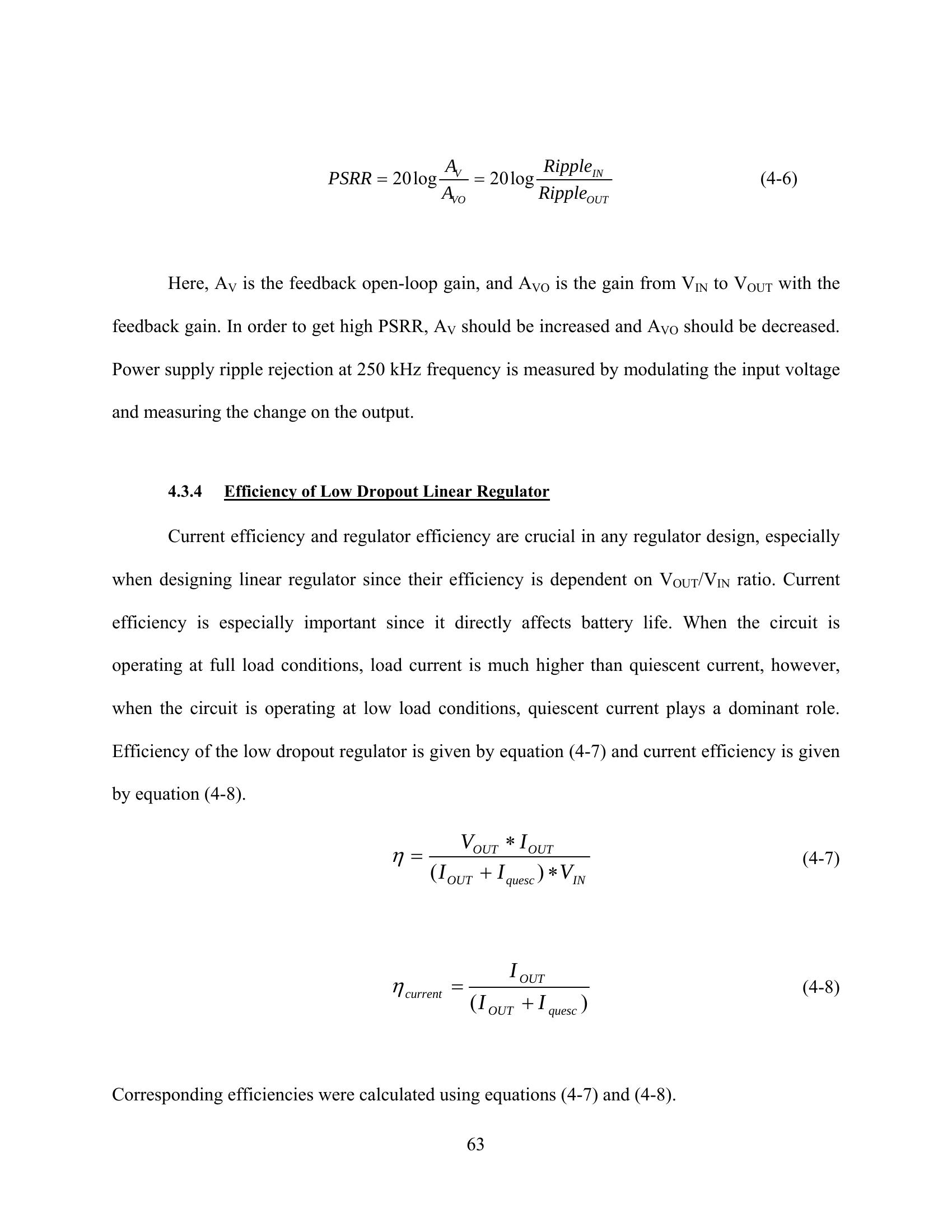
Table 2. LDO regulator efficiency
Block V V I I η
IN OUT OUT quiescent
DRAM 1.8V 1.5V 30mA 42uA 83%
DSP 1.5V 1.2V 70mA 35uA 80%
Sensor 1.2V 1.0V 4mA 31uA 82%
As seen from the results in Table 2, efficiency of the on-chip low dropout regulators is above
80%, which is good considering other benefits provided by the LDO such as low cost, small
area, and simplicity of the design.
4.4 Simulation Results and Analysis
The two-stage design simulations are performed using SPICE simulation tool. First,
stage-1 consisting of a switching regulator, Figure 4-16, is simulated and analyzed. The buck-
type switching regulator steps down an input voltage of 3.7V to an output voltage of 1.8V.
Buck
V Switching V
IN OUT
Regulator
Control Input
Figure 4-16. Stage-1, switching regulator
64
| Block | V IN | V OUT | I OUT | I quiescent | η |
| DRAM | 1.8V | 1.5V | 30mA | 42uA | 83% |
| DSP | 1.5V | 1.2V | 70mA | 35uA | 80% |
| Sensor | 1.2V | 1.0V | 4mA | 31uA | 82% |
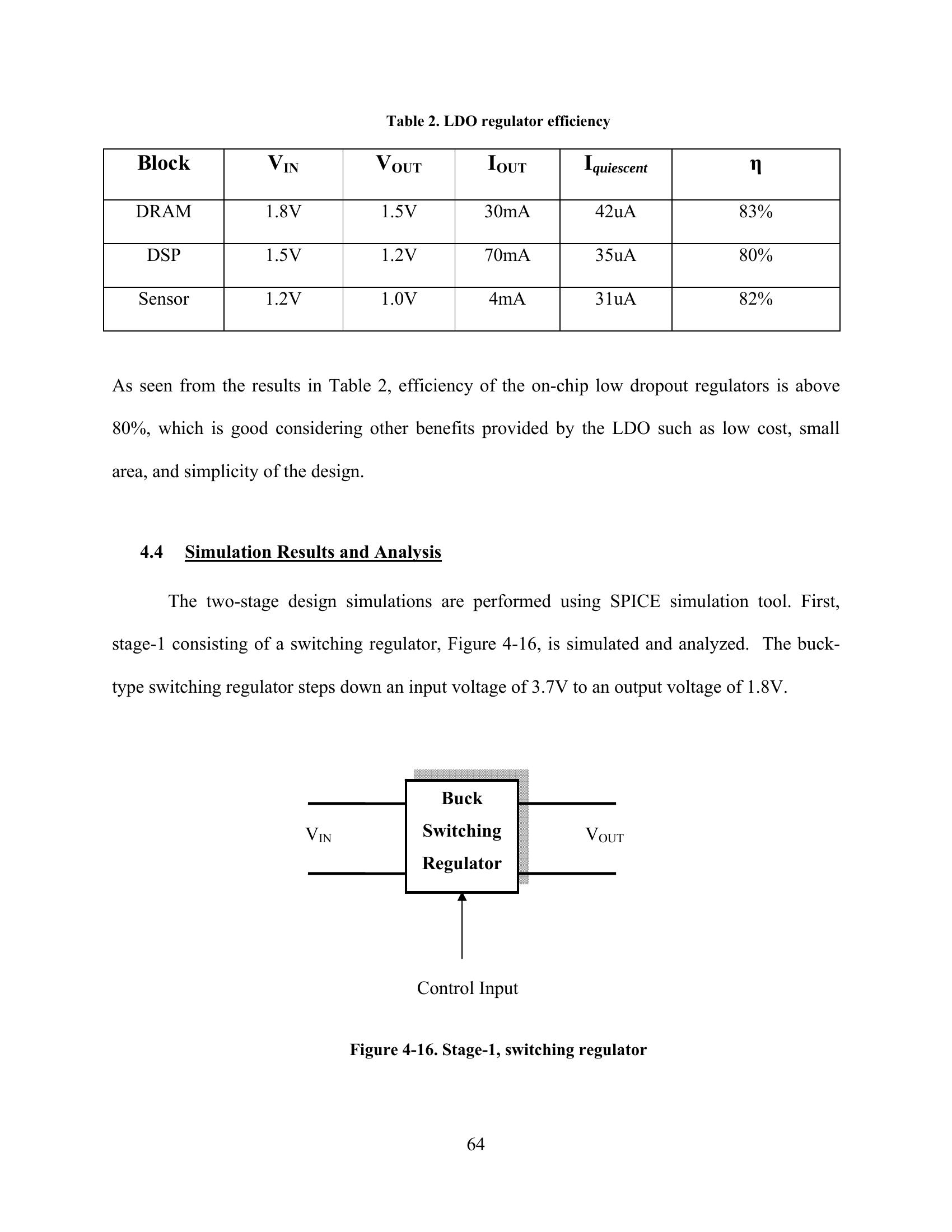
Simulations were performed to verify minimal output voltage dependency on the load.
Loads in the interval from no-load to a 10-Ohm load resistance were selected and the results are
shown in Figure 4-17. In the figure, a 3.7V input is shown along with other voltage waveforms.
When there is no load in circuit the output resembles the input with a very small ripple due to
switching. Furthermore, examining the curves corresponding to various loads, their effect is
shown on the output waveform. Higher load experiences more ripple. However, despite the
ripple, the waveform stabilizes and approaches the desired output of 1.8V after about 1ms.
Figure 4-17. Switching regulator output waveforms
65
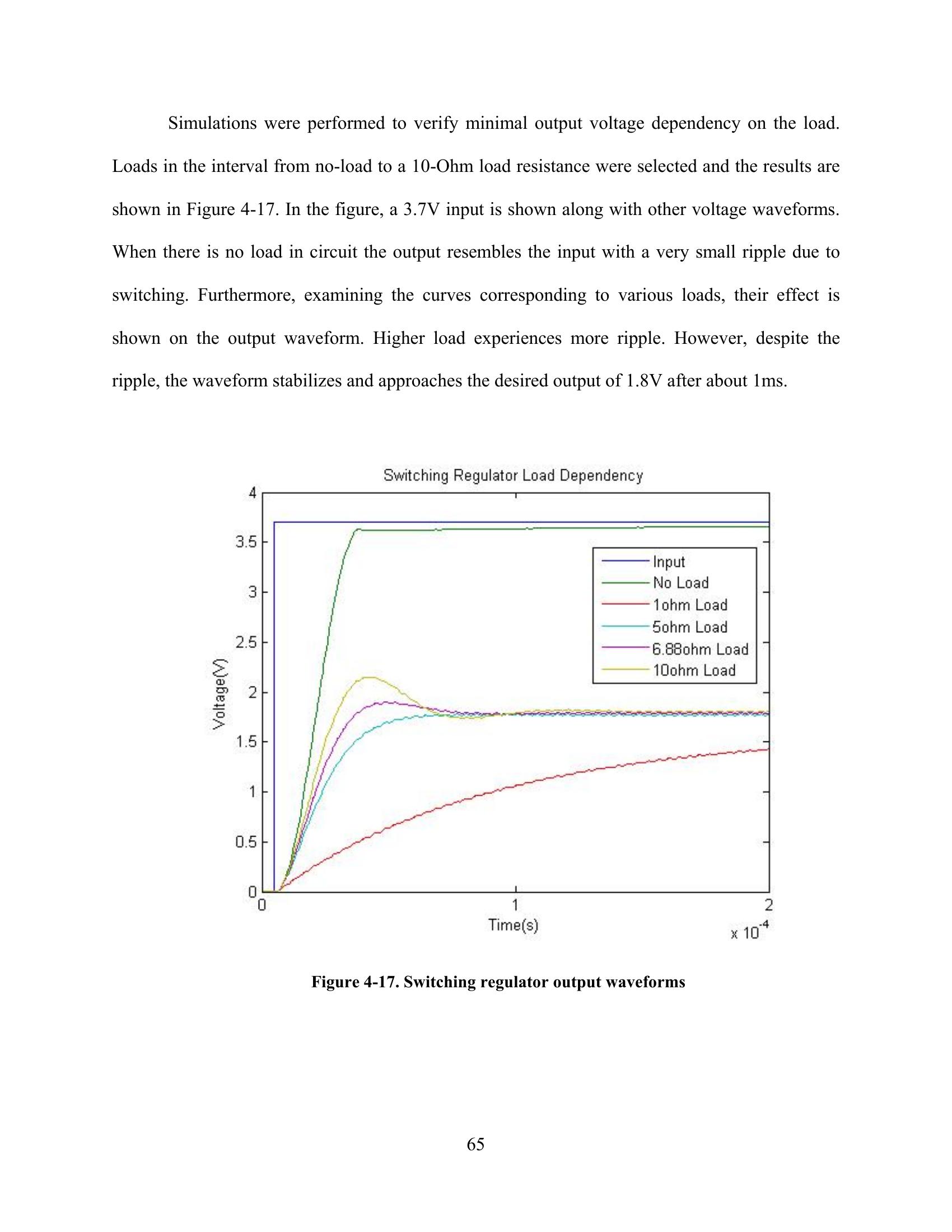
Transient response of a variable load, a varistor, is shown in Figure 4-18 and as expected
after any load change output voltage experiences a small ripple then stabilizes to the desired
value.
Figure 4-18. Transient response
After an efficient switching regulator first stage was designed, it was used as the source
for the building block of the tree design, shown in Figure 4-19. The results of the building block
consisting of the switching regulator source and the LDO second stage are shown in Figure 4-20.
The simulations are performed for a DRAM load operating at 1.5V. Graphs in Figure 4-20 show
the response of the quiescent current of the LDO as well as its input and output voltages to the
load current change.
66
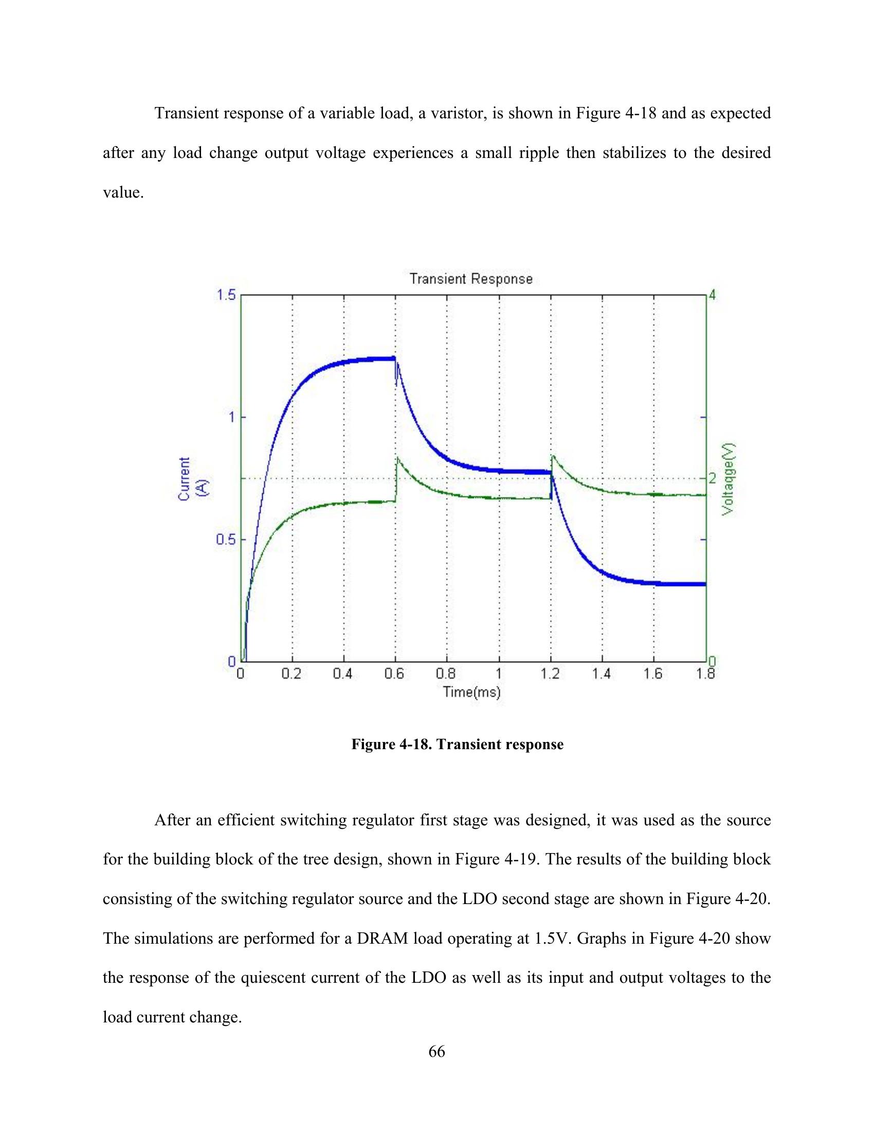
Buck
LDO
Switching
3.7V 1.8V 1.5V
Regulator Regulator
Control Input
Figure 4-19. Switching-LDO building block
Figure 4-20. Switching-LDO building block waveforms
67
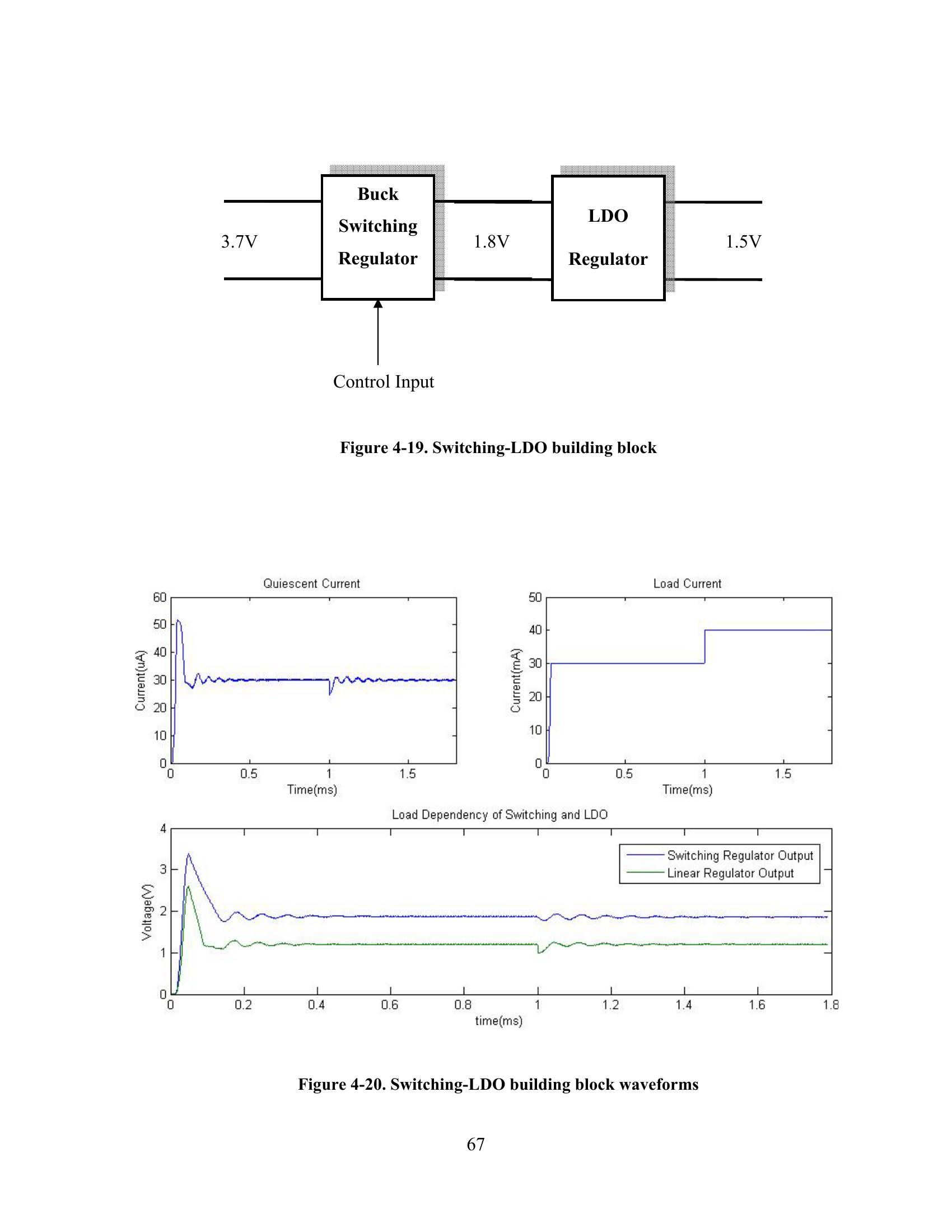
As the load current consumption increases about 30%, both voltages experience small
ripple and settle to the same designed voltages. The size of the ripple has a direct relation with
the time and value of the load current transient. When the transient has a bigger step such as at
the input, the ripple is higher. However, when the step is relatively small such as the load
transient increasing from 30-40mA, the ripple is lower.
Using the previous results of the main building block of the design, two more additional
branches were added, as shown in Figure 4-21 followed by simulation results in Figure 4-22.
Corresponding voltages and currents were measured.
Supply
DRAM @1.5V,
Switching LDO0
30mA
Regulator
DSP @1.2V,
LDO1 70mA
Sensor @1.0V,
LDO2 4mA
Figure 4-21. Switching-LDO tree design
68
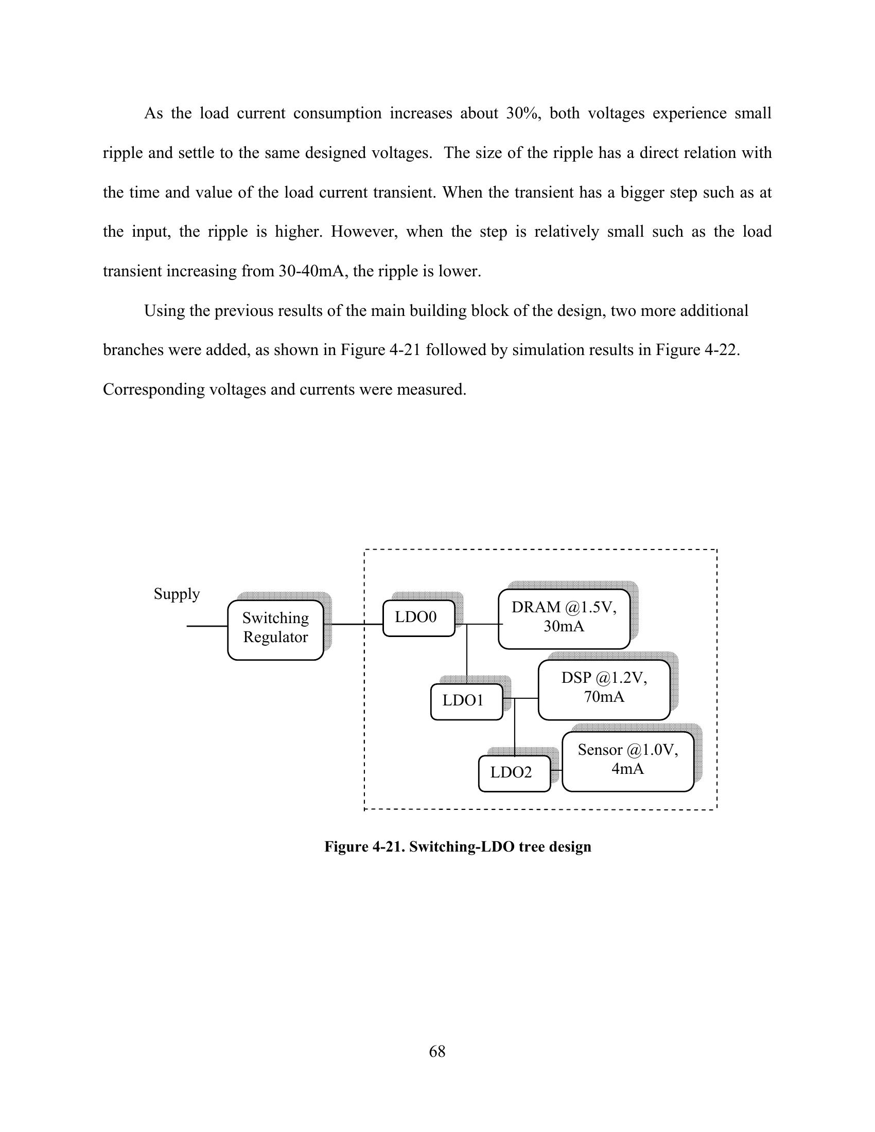
Figure 4-22. Switching-LDO tree design waveforms
As seen in Figure 4-22, the highest ripple is experienced at the input of the first branch. Other
branches inherit this as well, however, the LDO has the ability to reduce ripple and since these
voltages go through multiple LDO branches the ripple effect is smaller.
69
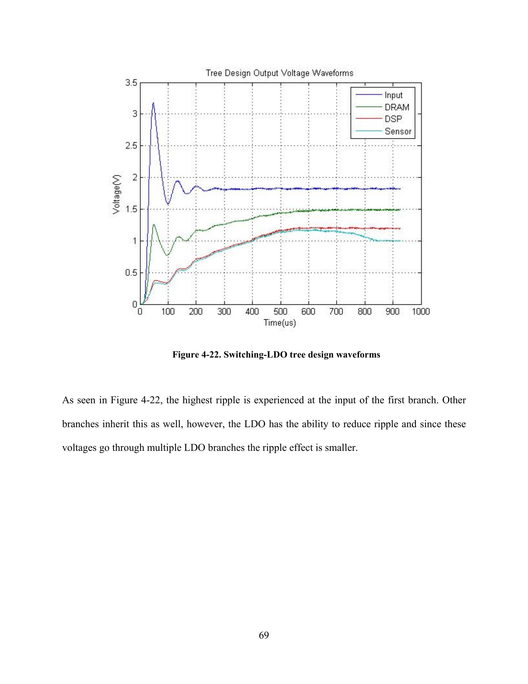
Figure 4-23. Switching-LDO tree design quiescent waveforms
Quiescent currents (ground currents) of all three LDO branches are shown in Figure 4-23. It is
imperative that their values remain small for maximum efficiency. In order to maintain small
quiescent current, a larger feedback resistor (R2=30K) was used.
The LDO branch response to changes in load current is shown in Figure 4-23. The
DRAM is increasing current consumption from 30mA to 35mA after 1ms, the DSP is decreasing
current consumption from 70mA to 65mA after 1.5ms, and the sensor is increasing current
consumption to about 10mA at about 3.3ms. As seen in the graphs each change in load current
causes changes in all the branches.
70
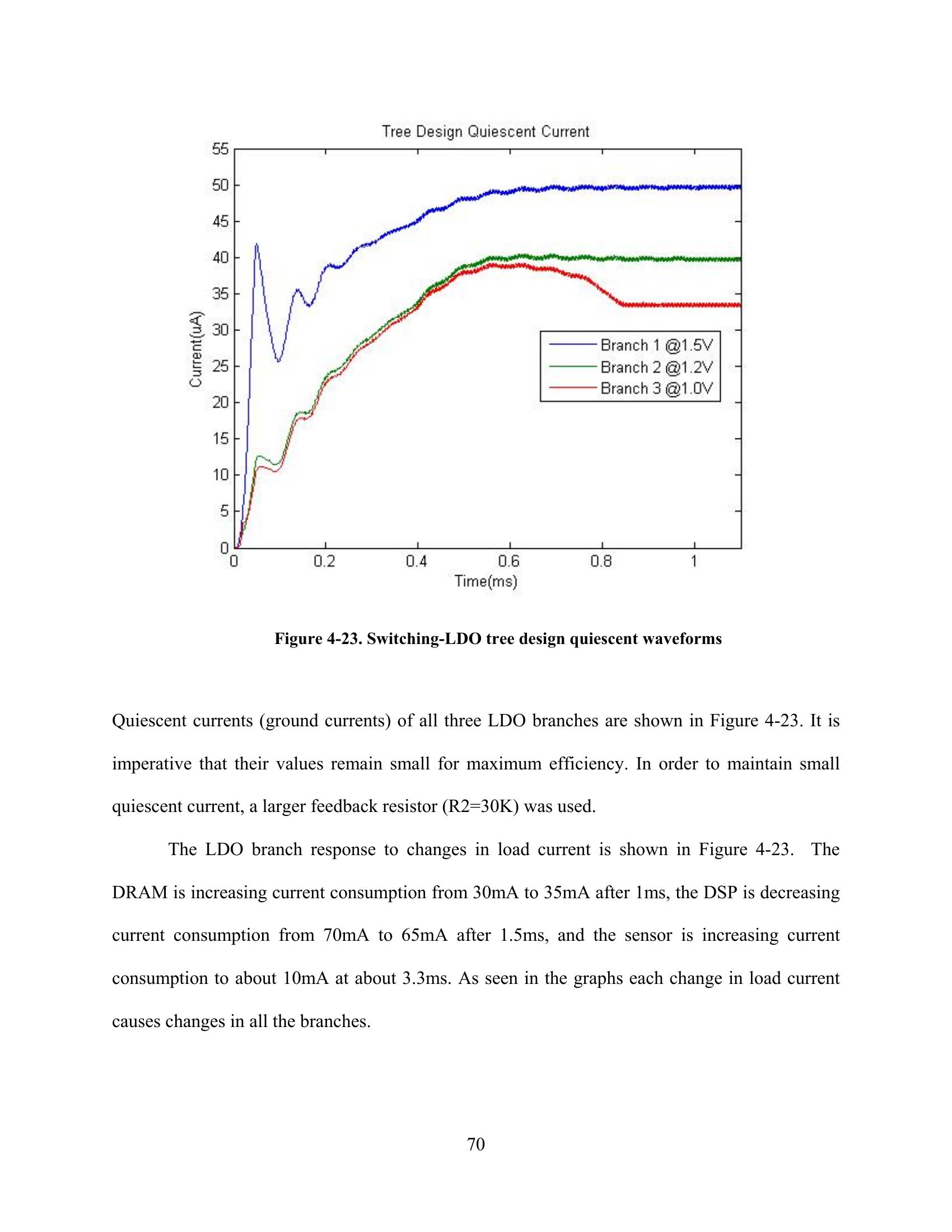
Figure 4-24. Switching-LDO tree design load transient waveform
71
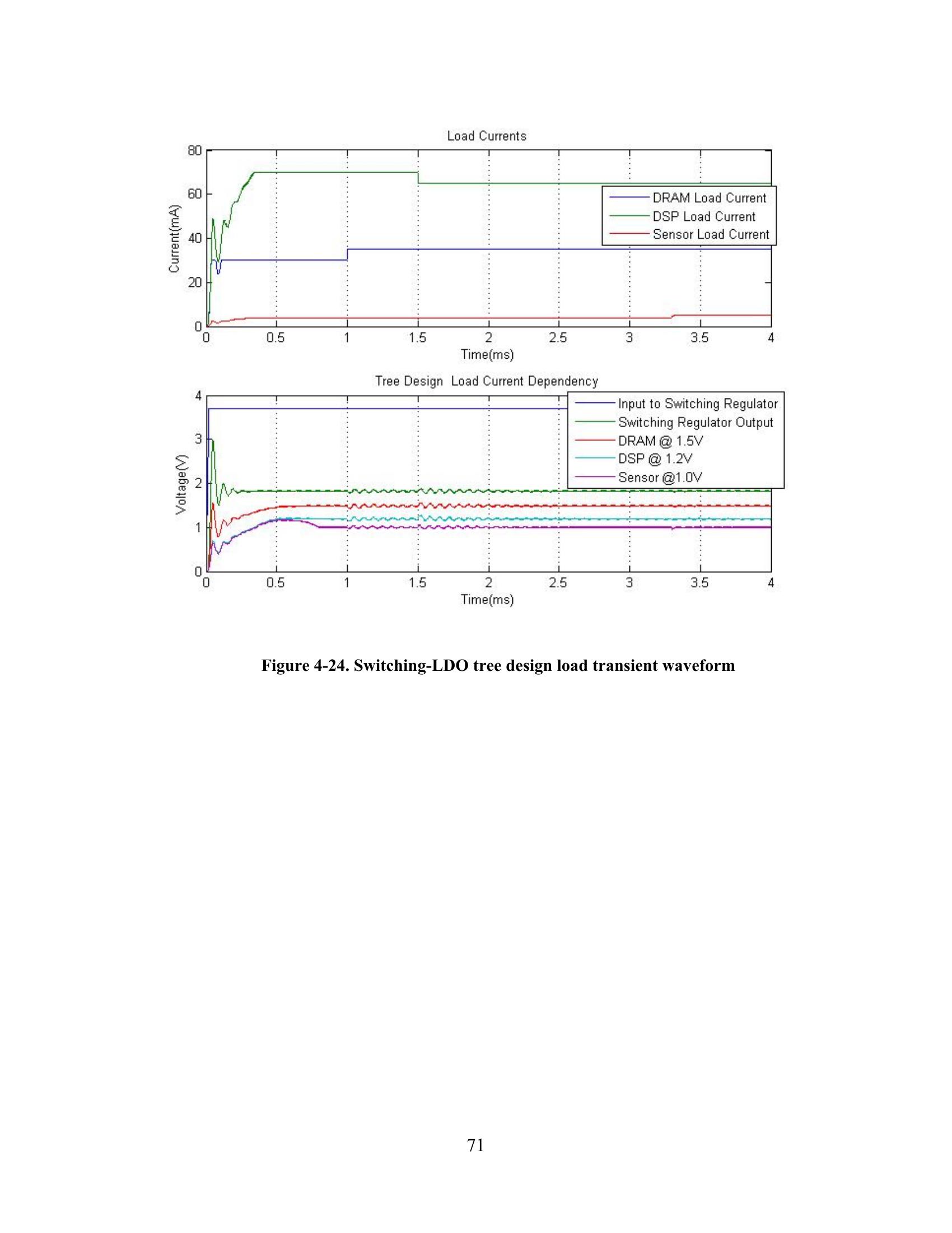
For comparison and proof of concept, a two-stage regulator was designed with the same
specifications, except this time the LDOs have the same 1.8V input source and are connected
parallel, as shown in Figure 4-25.
Supply
DRAM @1.5V,
Switching LDO0
30mA
Regulator
DSP @1.2V,
LDO1
70mA
Sensor @1.0V,
LDO2
4mA
Figure 4-25. Switching-LDO tree design
Figure 4-26 shows the effect that a higher input voltage has on efficiency and performance of the
LDOs. Since the dropout across the regulator is higher, the efficiency decreases and therefore
there is more heat dissipation in the system. In addition, it is important to mention that all the
output voltages experience more ripple than in the previous tree design, however they still
stabilize to the desired output level.
72
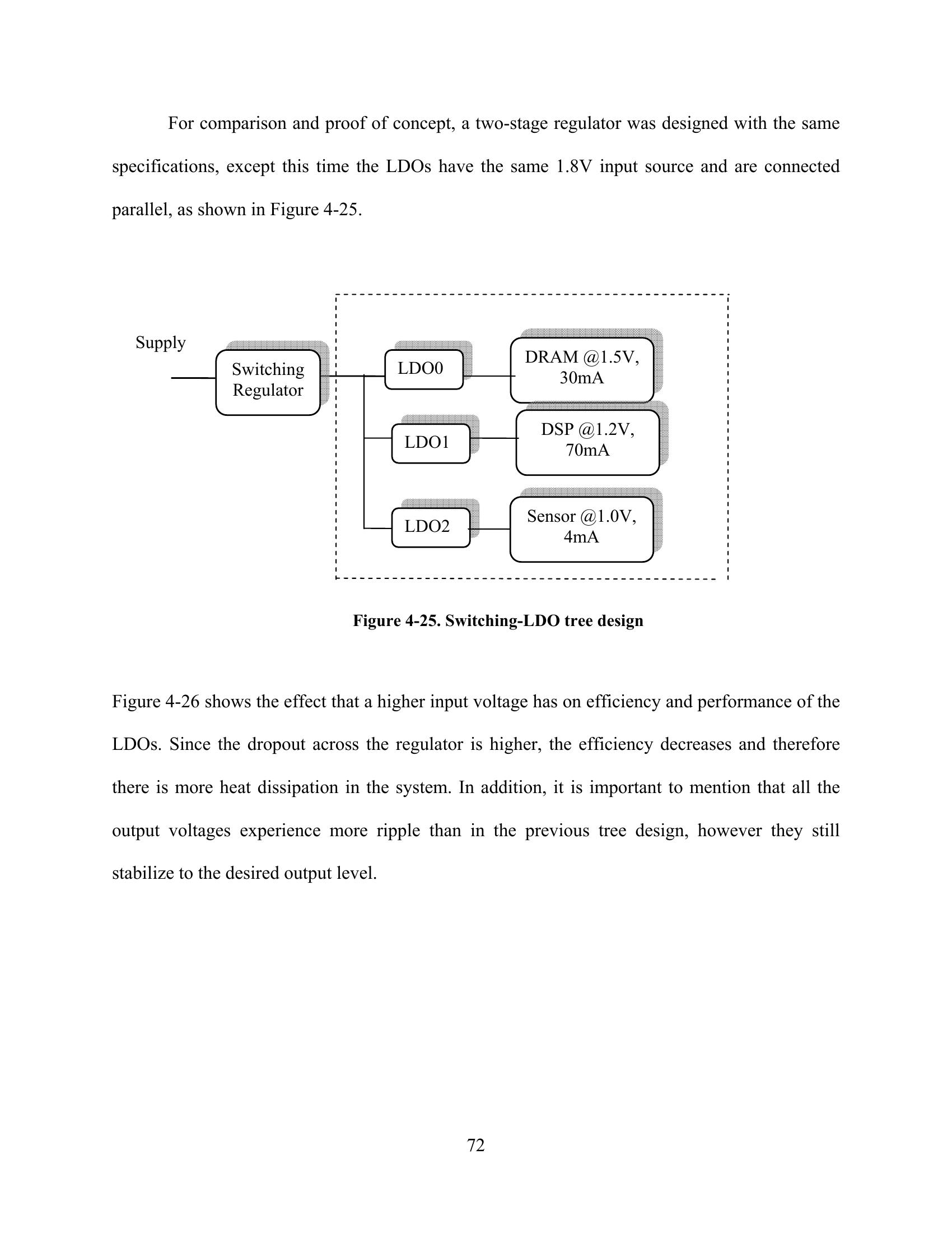
Figure 4-26. Switching-LDO parallel design waveforms
Table 3. LDO regulator efficiency, parallel design
Block V V I I η
IN OUT OUT quiescent
DRAM 1.8V 1.5V 30mA 49uA 83%
DSP 1.8V 1.2V 70mA 39uA 67%
Sensor 1.8V 1.0V 4mA 34uA 56%
Results in table 3, show that efficiency of the LDO degrades with the increase in dropout
voltage. The more voltage is dropped across the regulator, the lower it efficiency becomes and
there is more power dissipation in the system.
73
| Block | V IN | V OUT | I OUT | I quiescent | η |
| DRAM | 1.8V | 1.5V | 30mA | 49uA | 83% |
| DSP | 1.8V | 1.2V | 70mA | 39uA | 67% |
| Sensor | 1.8V | 1.0V | 4mA | 34uA | 56% |
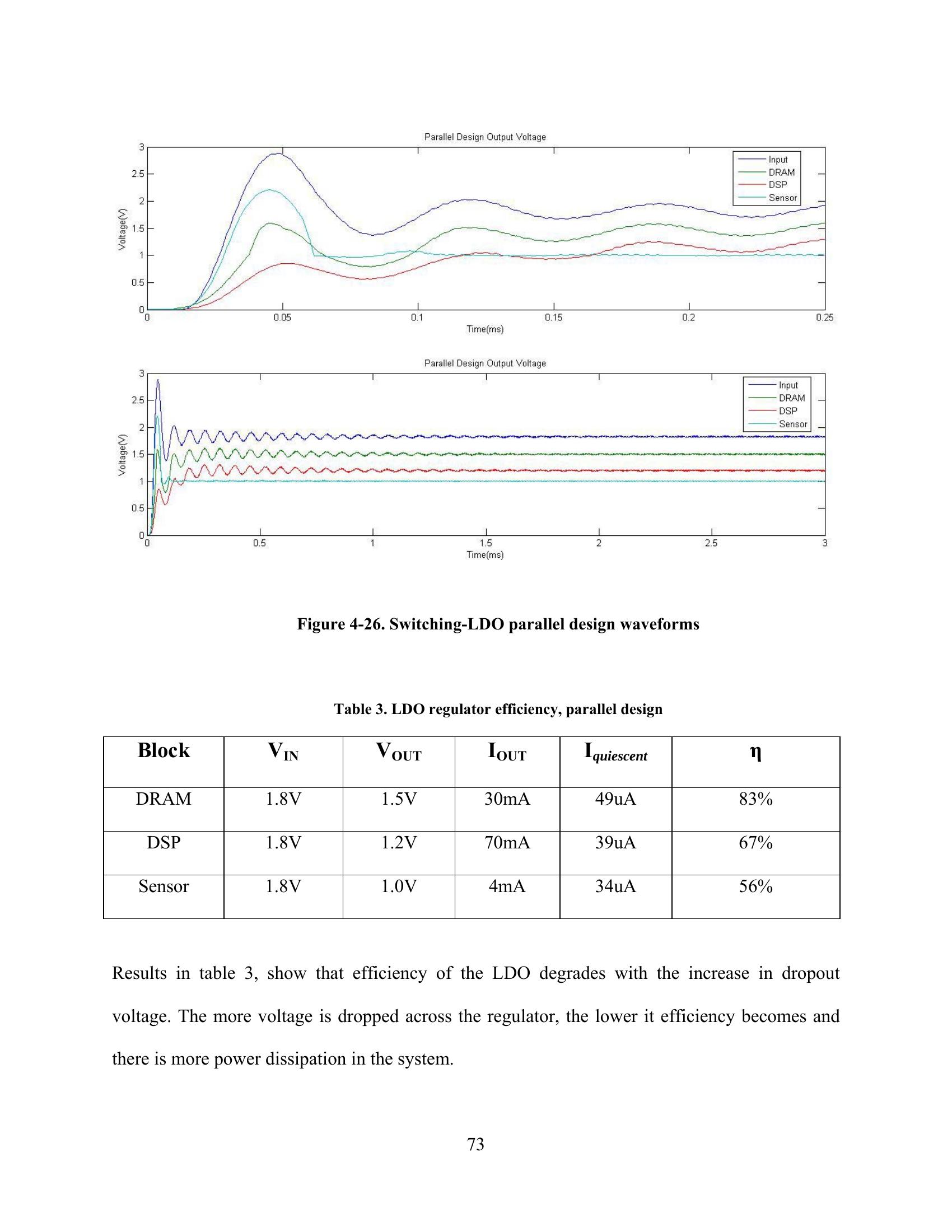
5 FUTURE WORK
In the future we are planning to continue this research and acquire a better understanding
of the hybrid structure. Future work includes optimization of the current two-stage approach, the
design of a good and efficient control system that will monitor both stages at the same time and
provide well-regulated voltage accordingly. Furthermore, this design will be optimized for high
current applications such as future multi-core processors operating with very low voltages and
very high currents in the range 50A-100A. This includes a current boosting technique that will be
placed at the output stage of the LDOs and increase current according to the system
specifications. The optimized design will be placed in a multi-core environment for power
management and distribution as well as for improved thermal stability. Sections 5.1 and 5.2
cover the initial work that our group has done in this direction.
5.1 Power Management and Thermal Stability in Multi-Core Chips
Due to the dramatic increase of power consumption and temperature it is not possible to
optimize the power profile and thermal stability just by attacking the problems from device,
interconnect or circuit levels. Rather a complete system level approach is required. PIs and their
groups plan to investigate the prospects of a self-sustainable thermal and power management
system design as outlined in Figure 5-1. In this planed multi-core dynamic power and thermal
management system we assume that all the state-of-the-art circuit and architecture level leakage
and power reduction techniques would already be implemented in those cores and other circuit
blocks. Still, it will be very crucial to monitor thermal stability of every component. One
74
sequence might cause one component to be used for long time. That might raise the temperature
of that particular component higher than the threshold value, which could jeopardize its
functionality. And failure of one component leads to the failure of the entire system. Therefore, a
mechanism to ensure the thermal stability of every component by controlling power consumption
in the system is essential. The developed voltage regulation scheme can play the central role in
this scheme.
Figure 5-1. Multi-core/multi-block Dynamic Power Management System
In the conceptual scheme, there are four cores, which are powered by the single voltage
regulated module (VRM). Four P-N junction sensors have been used to sense the temperature of
the cores, and those temperature signals are transferred to the signal conditioning & ADC
module, which will convert the signals into some values and will pass it to the logic circuits for
comparison with the threshold values. If any of the values surpasses the threshold value, the
75
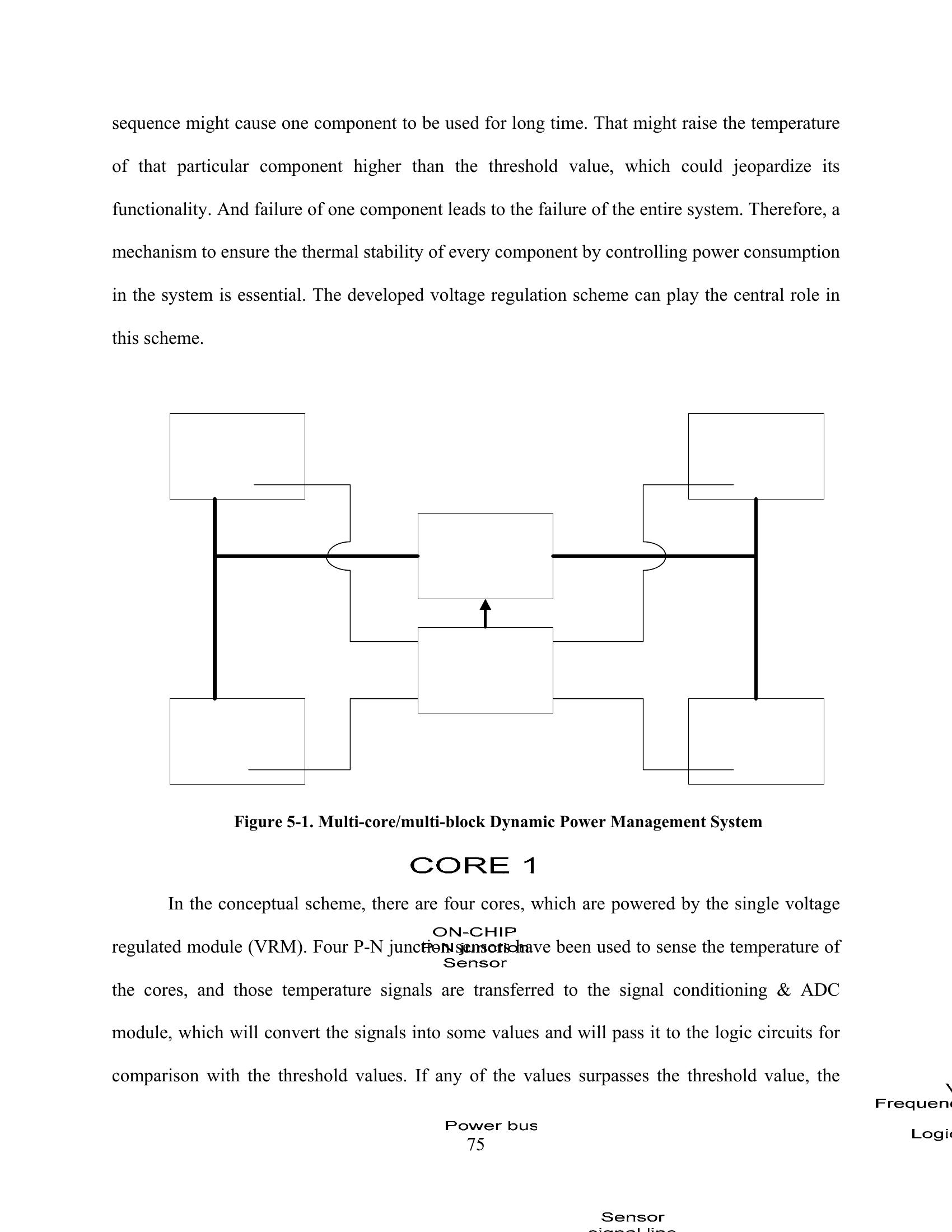
VRM will be notified and VRM/Frequency regulator will activate the power gating structures for
that particular core. In this way, the entire system is going to be self-sustained without any
external monitoring. Along with it, we can always implement all existing power management
techniques like timeout. But as long as the proposed mechanism is there, a run-time control of
thermal stability can be achieved. Figure 5-1 provides a conceptual overview of the proposed
scheme. At this stage the focus is not to develop circuit techniques for implementing VRM for
this self-sustained control. However, the initial goal is to synthesize the policy for such control,
and identify relevant research needs so that long-term research projects can be undertaken for
successful implementation of reconfigurable multi-core SOC thermal and power management.
5.2 Efficient Power Gating Techniques for Multi-Core Design
To implement the above power management and thermal stability scheme an efficient
power gating is required to balance between the activities and power consumptions in various
circuits or core clusters. In [30]-[32], our group proposed an innovative power gating technique
that can be adopted in single-core and multi-core SOCs. The underlying concept of the proposed
technique is illustrated in Figure 5-2.
76

VDD
Sleep/clock
Control
transistor
VVDD
Logicor memory Parallel gating path with
circuit/block/core switching device(s)
VGND
Sleep/clock Control
transistor
GND
Figure 5-2. The Proposed Power Gating Scheme
In the proposed scheme an additional power gating path is provided in parallel to
conventional sleep transistors used for power gating or clock transistors used in dynamic circuits.
This parallel power gating path will contain single or multiple switching devices depending the
expected leakage reduction and allowable reliability tolerance. The combination of sleep/clock
transistors and accompanying parallel current paths will be placed in between real and virtual
supply rails, while the logic or memory circuit/block/core will be placed in between virtual
supply rails. The control of the operation of these parallel paths can be exactly similar to that of
sleep/clock transistors, or the control can be incorporated with a dynamic run-time observation of
certain metric of the circuits or systems. Here, we propose to control the operation of this power
gating scheme based on the run-time estimation of spatial thermal profile of the
circuits/blocks/cores under consideration. Whatever the control mechanism, the purpose of
adding these additional power gating paths is to provide three modes – active (RUN),
intermediate data-retention (HOLD) and cut-off.
77
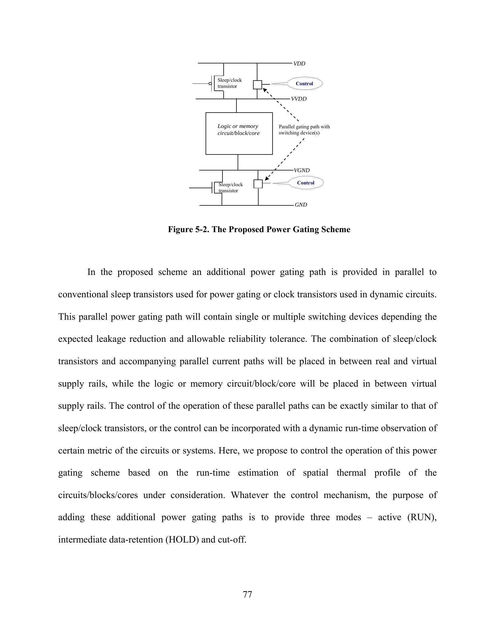
While regular sleep/clock transistors are off various levels of leakage and ground bounce
reduction can be achieved by shifting to HOLD or cut-off modes. In the RUN mode these
parallel paths provide additional operating currents, thereby improving performance of the
circuits or systems. The HOLD mode will act as data retention mode, thus eliminating the need
for additional data recovery circuitry. Selection and arrangement of switching devices will
ensure how much control on leakage and ground bounce can be achieved. In this HOLD mode
the voltage across the virtual rails will be reduced by an amount equal to multiple threshold
voltages of the switching devices used. Since, the effective voltage across the logic circuit is
reduced the overall leakage current will be reduced in this mode. If a complete suppression of
power consumption is necessary during long idle period a transition to cut-off mode can be
made. During the return of the circuit from cut-off to RUN mode the HOLD mode can be
employed as intermediate state to control ground bounce noise in power delivery system.
In our group’s recent publications, [30]-[32], two different implementations of the
proposed concept are presented. In these implementation MOS transistors and MOS diodes are
used as switching devices, which provide multiple-VTH reduction of effective voltage across the
logic circuits/cores during the idle mode. Here, the number of series MOS diodes is a design
variable to manage the leakage-recovery time tradeoff. However, a greater freedom would be
highly desirable in setting the VVDD/VGND voltage. Indeed, a finer granularity would be useful
– not only multiples of VTH (consider that 2VTH is almost VDD, in sub-100 nm technologies).
Moreover, it would be useful to set VVDD/VGND independently of the variations in the switch
transistors. This can be done by setting VVDD/VGND with an Op-Amp driving the gate or bulk
voltage of the added power switches, according to a desired reference voltage VREF. In this
way, we have two degrees of freedom when driving the power switch: this allows for also
78
reducing the switch leakage, once VVDD/VGND is assigned (for example, Reverse Body
Biasing may be used to reduce the switch leakage during the intermediate standby, and Reverse
Gate Biasing may be used to reduce the switch leakage in standby or normal operation). The
above mechanisms are suitable for dynamic operation, changing VREF according to the
instantaneous leakage-recovery tradeoff at the considered point of time.
Furthermore, our future work will include the design of an inductor-less switching
regulator option that can be integrated on the same chip as the load without size, cost, and
efficiency constraints. Inductors have always been a bottleneck in nano- and micro-electronic
circuits due to their relatively large size, their tendency to pick up noise in the electromagnetic
spectrum as well as difficulty to fabricate and interface with CMOS and BJT devices. In general,
inductive effects are dampened by resistance but at high frequencies and wide and long lines
inductance may cause delays, noise, and other signal integrity problems. Difficulty with on-chip
inductance is also result of current return paths that are difficult to figure out and wires may
influence each other even if they are not close.
We have done some initial work in designing inductor-less switching regulators and will
continue our research further. For on-chip regulators, using inductor-less option does not help the
case since there is still lack of efficiency and good regulation capacity. Therefore, instead we use
simulated inductors to replace real inductors. Before replacing the inductor in a regulator circuit
it is important to notice that the inductor is floating and not earthed. Therefore, it can be replaced
by circuitry that simulates a floating inductor.
Through circuit techniques, an inductor may be simulated with a capacitor and linear
active devices. However, the linear active devices will be very inefficient, making an inductor
that is using a lot of power not necessarily as a parasitic resistance in the inductor, but still
79

wasting energy somewhere. Such circuits can be gyrators realized with resistors, capacitors, and
active devices such as operational amplifiers. Therefore, gyrator implementation with
transconductors is preferred. Furthermore, gyrators consist of two voltage controlled current
sources whereas operational amplifiers are voltage controlled voltage sources, so to make the
implementation of the gyrator simpler we use transconductors [4]. The input impedance of the
gyrator is inversely proportional to the output impedance and therefore it allows the conversion
of a capacitor into an inductor.
Because a gyrator is fundamentally a connection of an inverting and non-inverting
voltage-controlled current source their implementation with transconductors is preferred over
operational amplifiers [4]. In [7] the realization of an inductor with a transconductance gyrator is
briefly discussed. Therefore, we performed initial simulations to show that this technique is
suitable for inductor replacement and that the gyrator behaves similarly to the inductor. Figure 5-
3 shows two gyrators back to back, one for each port that replace the inductor.
Figure 5-3. Switching regulator operating with transconductance gyrator
The value of inductance depends on the capacitor connecting the two gyrators and on the value
of tranconductance. This research work on on-chip power management and voltage regulation
will be followed by many optimization and improvements for a wide application range including
multi- and many-core systems.
80
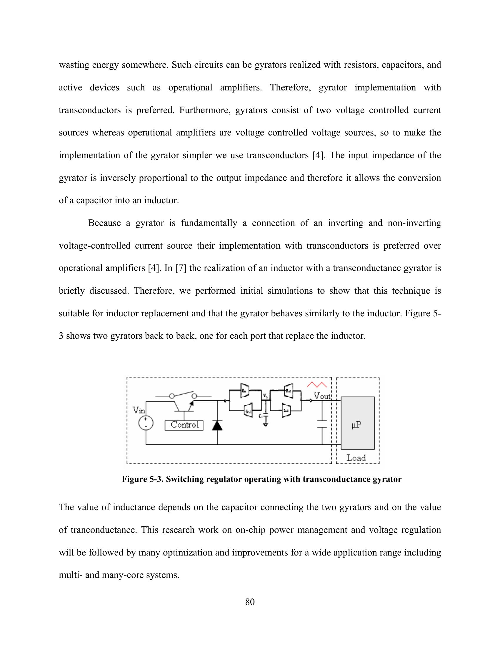
6 CONCLUSION
In this dissertation we have presented analysis and design of a two-stage voltage
regulator conversion that handles challenges coming from the input side and load side. The first
stage steps down the voltage from the power supply and the second stage steps it down to bring it
close to the level required by the load. This design deals with challenges faced by many circuit
and device designers in this new nanometer era.
The proposed methodology includes the first stage consisting of a switching voltage
regulator located off-chip and the second stage consisting of a tree low dropout linear regulator
topology located on-chip. The tree orientation assures low dropout across the regulator and
provides improved efficiency, fast transient response, and noise reduction. This technique
proves to be efficient, simple, and less costly compared to other options that offer total on-chip
integration of switching regulators. The proposed approach combines the advantages of both
voltage regulator topologies, switching and linear, and results in one hybrid design that is
suitable for multi-core SOC implementations and designs.
In addition, a hot swap controller is proposed, to limit undesirable inrush currents
experienced by power supplies at turn on due to switching elements. The results show that this
technique is effective in also protecting the load from voltage droops. The controller limits the
inrush current by slowly decreasing the on-resistance of the N-Channel MOSFET. It also
provides protection against high voltage transients and over- and under-voltage defects. When
the circuit starts powering up, circuit components have an immediate need to extract a large
transient current from the voltage source. The controller monitors this inrush current and slowly
enhances the MOSFET and allows the voltage at the MOSFET’s drain to rise from zero volts.
81
The current can be controlled by sensing the current across the resistor and controlling the gate
accordingly. After detailed analysis and simulations it is concluded that the two-stage tree
topology provides well-regulated voltage with high efficiency, higher that the conventional linear
regulator counterparts.
82

REFERENCES
[1] W. Kim, et. El, “Enabling On-Chip Switching Regulators for Multi-Core Processors
using Current Staggering,” Workshop on Architectural Support for Gigascale
Integration 2007, held in conjunction with ISCA 2007.
[2] W. Kim, et. El, “System Level Analysis of Fast, Per-Core DVFS using On-Chip
Switching Regulators,” 14th International Symposium on High-Performance
Computer Architecture, HPCA’08
[3] K. Waldschmidt, et. El, “Reliability-Aware Power Management of Multi-Core
Systems,” Dagstuhl Seminar Proceedings 06141, (2006).
[4] Franco, Sergio. “Linear and Switching Regulators.” Design with Operational
Amplifiers and Integrated Circuits. Ed. Director, Stephen W. New York: McGraw-
Hill, 2002. 499-557.
[5] M. Swaminathan, et. El, “Power Distribution Networks for System-on-Package:
Status and Challenges,” IEEE Transactions on Advanced Packaging, (2004).
[6] H. Feng, G. Jelodin, K. Gong, R. Zhan, Q. Wu and A. Wang. “Super Compact RFIC
Inductors in 0.18um CMOS with Copper Interconnects,” IEEE MTT-S Digest, vol. 4,
pp. 570-578, (2002).
[7] Y. Panov and M. Jovanovic. “Design Considerations for 12-V/1.5-V, 50-A Voltage
Regulator Modules,” IEEE Transactions on Power Electronics, 16(6), (2001).
[8] W. Wu, N. Lee, and G. Schuellein. “Multi-Phase buck Converter Design with Two-
Phase Coupled Inductors,” In IEEE Applied Power Electronics Conference and
Exposition, (2006).
[9] S. Abedinpour, et. El, “A Multi-Stage Interleaved Synchronous Buck Converter with
Integrated Output Filter in a 0.18um SiGe Process,” In IEEE International Solid State
Circuits Conference, (2006).
[10] G. Schrom, et. El, “A 480-MHz, Multi-Phase Interleaved Buck DC-DC Converter
with Hysteretic Control,” In IEEE Power Electronics Specialist Conference, (2004).
REFERENCES (continued)
83
[11] Int. Technology Roadmap for Semiconductors (ITRS) (2003).
[12] J. Clarkin, “Design of a 50A Multi-Phase Converter,” in Proc. Conf. Rec., HFPC, pp.
414–420, (1999).
[13] R. Bergamaschi, et. El, “Exploring Power Management in Multi-Core Systems,”
Design Automation Conference, Asia and South Pacific, pp. 708–713, (2008).
[14] A. Makharia and G. A. Rincon-Mora. “Integrating Power Inductors onto the IC-SOC
Implementation of Inductor Multipliers for DC-DC Converters,” Industrial
Electronics Society, the 29th Annual Conference of the IEEE, vol. 1, pp. 556-561,
(2003).
[15] P. Hazucha, T. Karnik, B.A Bloechel, C. Parsons, D. Finan, and S. Borkar, “Area-
Efficient Linear Regulator With Ultra-Fast Load Regulation,” IEEE Journal of Solid-
State Circuits, Vol. 40, No. 4, (2005).
[16] T. Endoh, K. Sunaga, H. Sakuraba, and F. Masuoka, “An On-Chip 96.5% Current
Efficiency CMOS Linear Regulator Using a Flexible Control Technique of Output
Current,” IEEE Journal of Solid-State Circuits, Vol.36, No. 1, (2001).
[17] V. Telandro, A. Malherbe, H. Barthelemy, “On-Chip Voltage Regulator Protecting
Against Power Analysis Attacks,” IEEE International Midwest Symposium on
Circuits and Systems, Vol.2, pp. 507 – 511, (2006).
[18] C. Jia, B. Qin, Z. Chen, “A Linear Voltage Regulator for PLL in SOC Application,”
International Conference on Wireless Communications, Networking, and Mobile
Computing, pp. 1 – 4, (2006).
[19] T. Simunic, K. Mihic, and G. De Micheli, “Power and Reliability Management of
SOCs,” IEEE Transactions on Very Large Scale Integration Systems, Vol. 15, No. 4,
(2007).
[20] H. J. Shin, S. K. Reynolds, et al. “Low-Dropout On-Chip Voltage Regulator for Low-
Power Circuits,” IEEE Symposium on Low Power Electronics, pp. 76-77, (1994).
[21] M. Shen, J. Liu, L. Zheng, and H. Tenhunen, “Chip-Package Co-Design for High
Performance and Reliability Off-Chip Communications,” High Density Microsystem
Design and Packaging and Component Failure Analysis, pp. 31-36, (2004).
[22] H. Martinez, A. Conesa, “Modeling of Linear-Assisted DC-DC Converters,” 18th
European Conference on Circuit Theory and Design, pp. 611-614, (2007).
[23] X. Zhou, P. Wong, et al. “Investigation of Candidate VRM Topologies for Future
Microprocessors,” IEEE Transactions on Power Electronics, Vol. 15, No. 6, (2000).
REFERENCES (continued)
84
[24] H. Liu, W. Lee, and Y. Chang, “A Provably Good Approximation Algorithm for
Power Optimization Using Multiple Supply Voltages,” Design Automation
Conference, pp. 887-890, (2007).
[25] B. Amelifard, M. Pedram, “Optimal Selection of Voltage Regulator Modules in a
Power Delivery Network,” Design Automation Conference, pp. 168-173, (2007).
[26] M. Popovich, E. Friedman, M. Sotman, A. Kolodny, “On-Chip Power Distribution
Grids with Multiple Supply Voltages for High Performance Integrated Circuits,”
IEEE Transactions on Very Large Scale Integration Systems, Vol. 16, pp. 908-921,
(2008).
[27] M. Gupta, J. Oatley, et al. “Understanding Voltage Variations in Chip
Multiprocessors using a Distributed Power-Delivery Network,” Design, Automation
and Test in Europe Conference and Exhibition, pp. 1-6, (2007).
[28] D. Brooks, V. Tiwari, M. Martonosi, “Wattch: A Framework for Architectural Level
Power Analysis and Optimization,” Proceedings of the 27th International Symposium
on Computer Architecture, pp. 83-94, (2000).
[29] G.A. Rincon-Mora, PhD thesis, Georgia Institute of Technology, (1996).
[30] Pervez Khaled, Jingye Xu, and Masud H. Chowdhury, “Dual Diode-Vth Reduced Power
Gating Structure for Better Leakage Reduction”, Proc. of IEEE MWCAS, August 2007.
[31] Masud H. Chowdhury, Juliana Gjanci, and Pervez Khaled, “Innovative Power Gating
for Leakage Reduction”, Proceedings of The 2008 IEEE International Symposium on
Circuits and Systems (ISCAS) Seattle, WA, USA, May 18-21, 2008, Page(s) 1568-
1571.
[32] Pervez Khaled, Jingye Xu, and Masud H. Chowdhury, “Better Leakage Reduction by
Exploiting the Built-in MOSFET-Vth Characteristics”, Proceedings of Seventh IEEE
International Conference on Electro/Information Technology (EIT2007), May 17-20, 2007,
Page(s): 98-102
[33] X. Zhou, P. Xu, and F. C. Lee, “A Novel Current-Sharing Control Technique for Low
Voltage High-Current Voltage Regulator Module Applications,” IEEE Transactions
on Power Electronics, Vol. 15, No. 6, (2000).
[34] G.A.Naylor, “DSP And FPGA Based Bunch Current Signal Processing,” Proceedings
DIPAC, France, (2001).
[35] N. Gutierrez, “Hot Swapping with Confidence,” National Semiconductor.
REFERENCES (continued)
85
[36] G. Papafotiou, T. Geyer, M. Morari, “Model Predictive Control in Power Electronics:
A Hybrid Systems Approach,” Proc. Of the 44th Conference on Decision and Control,
and the European Control Conference, (2005)
[37] URL www.intel.com, “Evolution of Intel Microprocessors.”
[38] E. Stanford, “Power Technology Roadmap for Microprocessor Voltage Regulators,”
Applied Power Electronics Conference, (2004).
[39] K. Bhattacharyya, P. Mandal, “A Low Voltage, Low Ripple, on Chip, Dual Switch-
Capacitor Based Hybrid DC-DC Converter,” 21st International Conference on VLSI
Design, (2008).
[40] S. Yuan, and B. C. Kim, “Low Dropout Voltage Regulator for Wireless
Applications,” IEEE 33rd Annual Power Electronics Specialist Conference, pp. 421-
424, Vol.2, (2002).
[41] V. Balan, “A Low-Voltage Regulator Circuit With Self-Bias to Improve Accuracy,”
IEEE Journal of Solid-State Circuits, Vol. 38, No. 2, (2003).
[42] URL www.maxim-ic.com, “Regulator Topologies for Battery Powered Systems,”
January 31, 2001.
[43] “Battery Management and DC-DC Converter Circuit Collection,” Appendix A,
Maxim application note, 1993.
[44] P. Wong, F. C. Lee, P. Xu, and K. Yao, “Critical Inductance in Voltage Regulator
Modules,” IEEE Transactions on Power Electronics, Vol. 17, No. 4, (2002).
[45] URL www.ti.com, B. M. King, “Understanding the Transient Response of the
LDOs.”
[46] P. Hazucha, S. Moon, et al. “High Voltage Tolerant Linear Regulator With Fast
Digital Control for Biasing of Integrated DC-DC Converters,” IEEE Journal of Solid-
State Circuits, Vol. 42, No. 1, (2007).
[47] X. Yuan, X. Wu, M. Zhao and X. Yan, “A Smart Hot Swap Controller IC Design,”
IEEE Conference on Electron Devices and Solid-State Circuits, pp. 293-296, (2005).
[48] D. E. Lackey, P. S. Zuchowski, et al. “Managing Power and Performance for System-
on-Chip Designs Using Voltage Islands,” In Proc. of International Conference on
Computer Aided Design, pp. 195-202, (2002).
[49] P. Hazucha, G. Schrom, et al. “A 233-MHz 80%-87% Efficiency Four-Phase DC-DC
Converter Utilizing Air Core Inductors on Package,” in IEEE Journal of Solid-State
Circuits, (2005).
REFERENCES (continued)
86
[50] G. Patounakis, Y. Li, K. L. Shepard, “A Fully Integrated On-Chip DC-DC
Conversion and Power Management System,” IEEE Journal of Solid-State Circuits,
Vol. 39, No. 3, (2004).
[51] J. G. Kassakian, M. F. Schlecht, and G. C. Verghese, “Principles of Power
Electronics”. Ed. Addison-Wesley, (1991).
[52] URL www.ti.com, “Understanding power supply ripple rejection in linear
regulators,” J. C. Teel.
87
