CHAPTER – 4
Logic Functions and Gates
Representing numbers using transistors is one thing, but getting the
computer to do something with those numbers is an entirely different
matter. Digital circuitry is used to perform operations such as addition
or multiplication, manage data, or execute programs. This chapter
presents the circuitry that is the foundation of data manipulation and
management within a computer.
4.1 Logic Gate Basics
Unless you are an electrical engineer, an understanding of the
operation of transistors is unnecessary. One level above the transistors,
however, is a set of basic building blocks for digital circuitry. These
building blocks are called logic gates, and it is at this level that we will
begin our discussion.
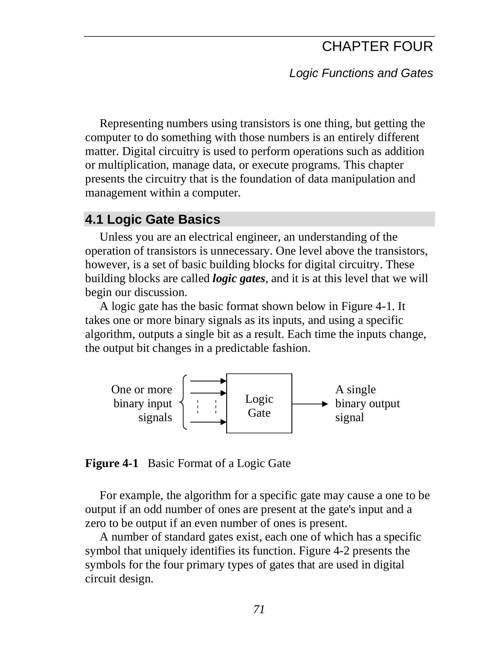
A logic gate has the basic format shown below in Figure 4-1. It
takes one or more binary signals as its inputs, and using a specific
algorithm, outputs a single bit as a result. Each time the inputs change,
the output bit changes in a predictable fashion.
One or more A single
Logic
binary input binary output
Gate
signals signal
Figure 4-1 Basic Format of a Logic Gate
For example, the algorithm for a specific gate may cause a one to be
output if an odd number of ones are present at the gate’s input and a
zero to be output if an even number of ones is present.
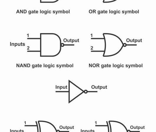
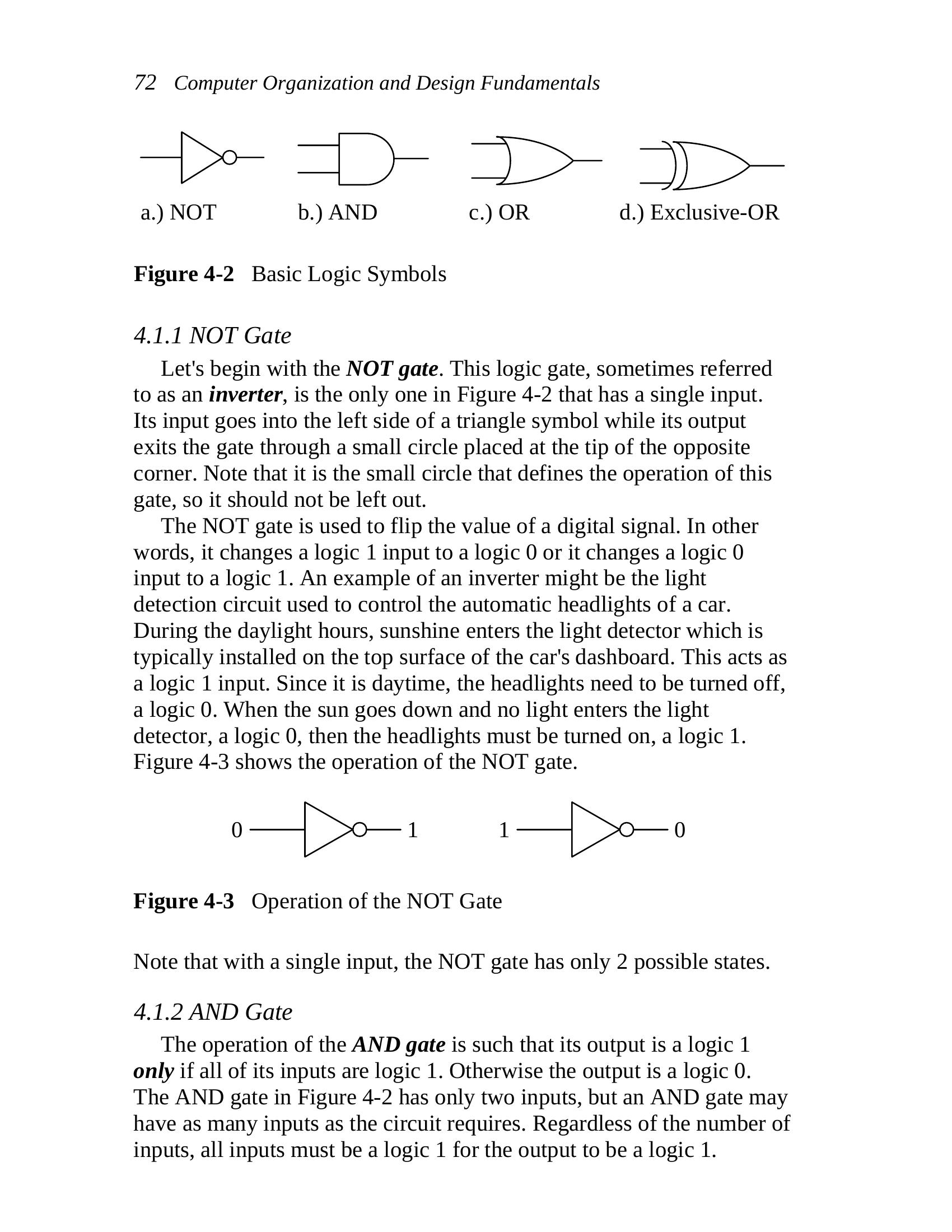
A number of standard gates exist, each one of which has a specific
symbol that uniquely identifies its function. Figure 4-2 presents the
symbols for the four primary types of gates that are used in digital
circuit design.
71
72 Computer Organization and Design Fundamentals
a.) NOT b.) AND c.) OR d.) Exclusive-OR
Figure 4-2 Basic Logic Symbols
4.1.1 NOT Gate
Let’s begin with the NOT gate. This logic gate, sometimes referred
to as an inverter, is the only one in Figure 4-2 that has a single input.
Its input goes into the left side of a triangle symbol while its output
exits the gate through a small circle placed at the tip of the opposite
corner. Note that it is the small circle that defines the operation of this
gate, so it should not be left out.
The NOT gate is used to flip the value of a digital signal. In other
words, it changes a logic 1 input to a logic 0 or it changes a logic 0
input to a logic 1. An example of an inverter might be the light
detection circuit used to control the automatic headlights of a car.
During the daylight hours, sunshine enters the light detector which is
typically installed on the top surface of the car’s dashboard. This acts as
a logic 1 input. Since it is daytime, the headlights need to be turned off,
a logic 0. When the sun goes down and no light enters the light
detector, a logic 0, then the headlights must be turned on, a logic 1.
Figure 4-3 shows the operation of the NOT gate.
0 1 1 0
Figure 4-3 Operation of the NOT Gate
Note that with a single input, the NOT gate has only 2 possible states.
4.1.2 AND Gate
The operation of the AND gate is such that its output is a logic 1
only if all of its inputs are logic 1. Otherwise the output is a logic 0.
The AND gate in Figure 4-2 has only two inputs, but an AND gate may
have as many inputs as the circuit requires. Regardless of the number of
inputs, all inputs must be a logic 1 for the output to be a logic 1.
Chapter 4: Logic Functions and Gates 73
As an example, picture a lamp that is connected to a plug in the wall
that is subsequently controlled by the light switch that is protected with
a circuit breaker. In order for the lamp to be on (logic 1), the switch at
the lamp must be on, the wall switch must be on, and the circuit breaker
must be on. If any of the switches turns to off (logic 0), then the lamp
will turn off. Another way to describe the operation of this circuit might
be to say, “The lamp is on if and only if the lamp switch is on and the
wall switch is on and the circuit breaker is on.” This should give you a
good idea of when an AND gate is used; just look for the use of the
word “and” when describing the operation of the circuit. Figure 4-4
shows all 22 = 4 states for a two-input AND gate.
0 0
0 0
0 1
1 1
0 1
0 1
Figure 4-4 Operation of a Two-Input AND Gate
4.1.3 OR Gate
An OR gate outputs a logic 1 if any of its inputs are a logic 1. An
OR gate only outputs a logic 0 if all of its inputs are logic 0. The OR
gate in Figure 4-2 has only two inputs, but just like the AND gate, an
OR gate may have as many inputs as the circuit requires. Regardless of
the number of inputs, if any input is a logic 1, the output is a logic 1.
A common example of an OR gate circuit is a security system.
Assume that a room is protected by a system that watches three inputs:
a door open sensor, a glass break sensor, and a motion sensor. If none
of these sensors detects a break-in condition, i.e., they all send a logic 0
to the OR gate, the alarm is off (logic 0). If any of the sensors detects a
break-in, it will send a logic 1 to the OR gate which in turn will output
a logic 1 indicating an alarm condition. It doesn’t matter what the other
sensors are reading, if any sensor sends a logic 1 to the gate, the alarm
should be going off. Another way to describe the operation of this
circuit might be to say, “The alarm goes off if the door opens or the
glass breaks or motion is detected.” Once again, the use of the word
“or” suggests that this circuit should be implemented with an OR gate.
74 Computer Organization and Design Fundamentals
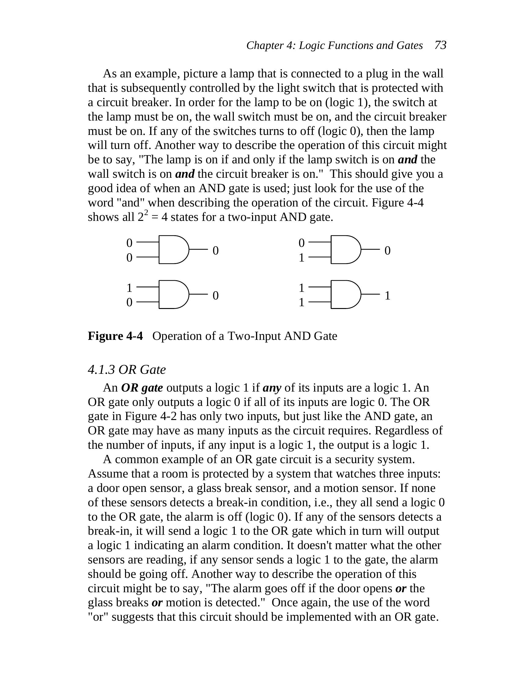
Figure 4-5 shows the 22 = 4 possible states for a two-input OR gate.
0 0
0 1
0 1
1 1
1 1
0 1
Figure 4-5 Operation of a Two-Input OR Gate
4.1.4 Exclusive-OR (XOR) Gate
An Exclusive-OR gate is sometimes called a parity checker. Parity
checkers count the number of ones being input to a circuit and output a
logic 1 or 0 based on whether the number of ones is odd or even. The
Exclusive-OR (XOR) gate counts the number of ones at its input and
outputs a logic 1 for an odd count and a logic 0 for an even count.
A common application for XOR gates is in error checking circuits.
If two digital signals are compared bit-by-bit, an error free condition
means that a logic 0 will be compared to a logic 0 and a logic 1 will be
compared with a logic 1. In both of these cases, there is an even
number of logic 1’s being input to the XOR gate. Therefore, as long as
the XOR gate outputs a logic 0, there is no error.
If, however, an error has occurred, then one signal will be logic 1
and the other will be a logic 0. This odd number of logic 1’s will cause
the XOR gate to output a logic 1 indicating an error condition.
Just as with the AND and OR gates, the XOR gate may have two or
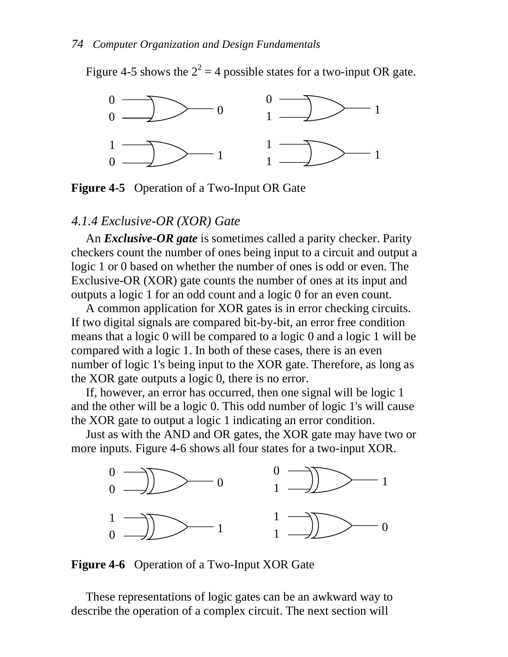
more inputs. Figure 4-6 shows all four states for a two-input XOR.
0 0
0 1
0 1
1 1
1 0
0 1
Figure 4-6 Operation of a Two-Input XOR Gate
These representations of logic gates can be an awkward way to
describe the operation of a complex circuit. The next section will
Chapter 4: Logic Functions and Gates 75
introduce an easier method for representing the operation of any digital
circuit incorporating the NOT, AND, OR, and XOR gates.
4.2 Truth Tables
The previous section described the operation of each logic gate with
words. This method isn’t efficient and is prone to misinterpretation.
What we need is a method to show the output of a digital system based
on each of the possible input patterns of ones and zeros.
A truth table serves this purpose by making a column for each of
the inputs to a digital circuit and a column for the resulting output. A
row is added for each of the possible patterns of ones and zeros that
could be input to the circuit. For example, a circuit with three inputs, A,
B, and C, would have 23 = 8 possible patterns of ones and zeros:
A=0, B=0, C=0 A=0, B=1, C=0 A=1, B=0, C=0 A=1, B=1, C=0
A=0, B=0, C=1 A=0, B=1, C=1 A=1, B=0, C=1 A=1, B=1, C=1
This means that a truth table representing a circuit with three inputs
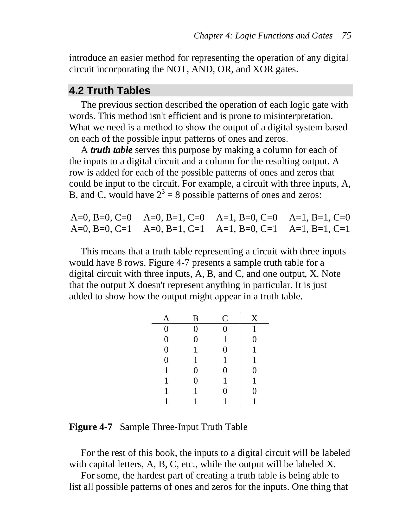
would have 8 rows. Figure 4-7 presents a sample truth table for a
digital circuit with three inputs, A, B, and C, and one output, X. Note
that the output X doesn’t represent anything in particular. It is just
added to show how the output might appear in a truth table.
A B C X
0 0 0 1
0 0 1 0
0 1 0 1
0 1 1 1
1 0 0 0
1 0 1 1
1 1 0 0
1 1 1 1
Figure 4-7 Sample Three-Input Truth Table
For the rest of this book, the inputs to a digital circuit will be labeled
with capital letters, A, B, C, etc., while the output will be labeled X.
For some, the hardest part of creating a truth table is being able to
list all possible patterns of ones and zeros for the inputs. One thing that
76 Computer Organization and Design Fundamentals
can help us is that we know that for n inputs, there must be 2n different
patterns of inputs. Therefore, if your truth table doesn’t have exactly 2n
rows, then a pattern is either missing or one has been duplicated.
There is also a trick to deriving the combinations. Assume we need
to build a truth table with four inputs, A, B, C, and D. Since 24 = 16, we
know that there will be sixteen possible combinations of ones and
zeros. For half of those combinations, A will equal zero, and for the
other half, A will equal one.
When A equals zero, the remaining three inputs, B, C, and D, will
go through every possible combination of ones and zeros for three
inputs. Three inputs have 23 = 8 patterns, which coincidentally, is half
of 16. For half of the 8 combinations, B will equal zero, and for the
other half, B will equal one. Repeat this for C and then D.
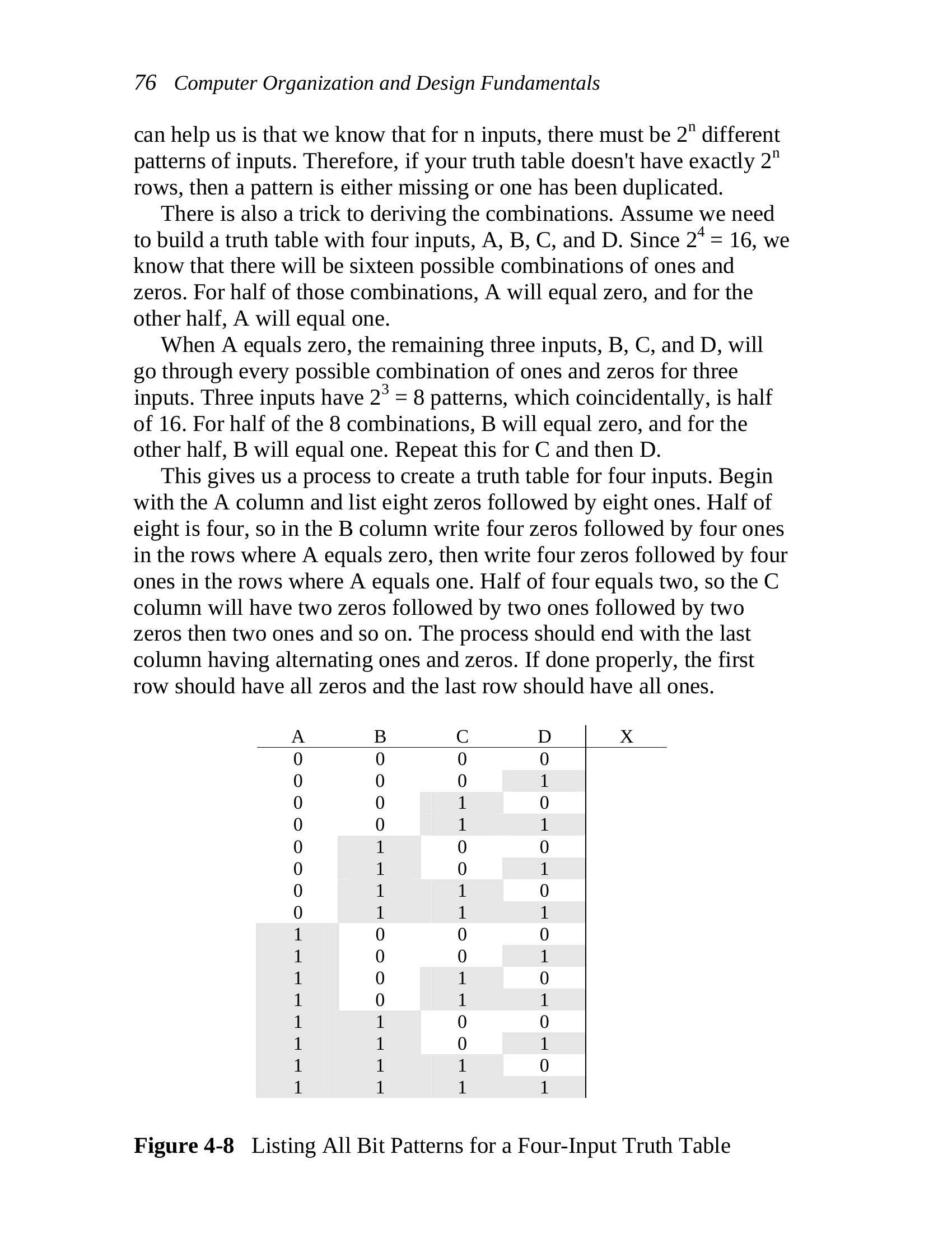
This gives us a process to create a truth table for four inputs. Begin
with the A column and list eight zeros followed by eight ones. Half of
eight is four, so in the B column write four zeros followed by four ones
in the rows where A equals zero, then write four zeros followed by four
ones in the rows where A equals one. Half of four equals two, so the C
column will have two zeros followed by two ones followed by two
zeros then two ones and so on. The process should end with the last
column having alternating ones and zeros. If done properly, the first
row should have all zeros and the last row should have all ones.
A B C D X
0 0 0 0
0 0 0 1
0 0 1 0
0 0 1 1
0 1 0 0
0 1 0 1
0 1 1 0
0 1 1 1
1 0 0 0
1 0 0 1
1 0 1 0
1 0 1 1
1 1 0 0
1 1 0 1
1 1 1 0
1 1 1 1
Figure 4-8 Listing All Bit Patterns for a Four-Input Truth Table
| None | None | None | None | None | None | None | None | None | None | |
| None | None | None | None | None | None | 1 | 0 | None | ||
| None | None | None | None | None | None | 1 | 1 | |||
| None | None | None | 1 | 0 0 0 1 | None | None | None | None | ||
| None | None | None | 1 | None | None | None | None | |||
| None | None | None | 1 | 1 | 0 | None | ||||
| None | None | None | 1 | 1 | 1 | |||||
| 1 | 0 0 0 0 0 1 0 1 0 0 1 1 | None | None | None | None | None | None | None | ||
| 1 | None | None | None | None | None | None | None | |||
| 1 | None | None | None | 1 | 0 | None | ||||
| 1 | None | None | None | 1 | 1 | |||||
| 1 | 1 | 0 0 0 1 | None | None | None | None | ||||
| 1 | 1 | None | None | None | None | |||||
| 1 | 1 | 1 | 0 | None | ||||||
| 1 | 1 | 1 | 1 |
Chapter 4: Logic Functions and Gates 77
In addition to verifying that all combinations of ones and zeros have
been listed, this method also provides a consistency between all truth
tables in the way that their rows are organized.
Now let’s use truth tables to describe the functions of the four basic
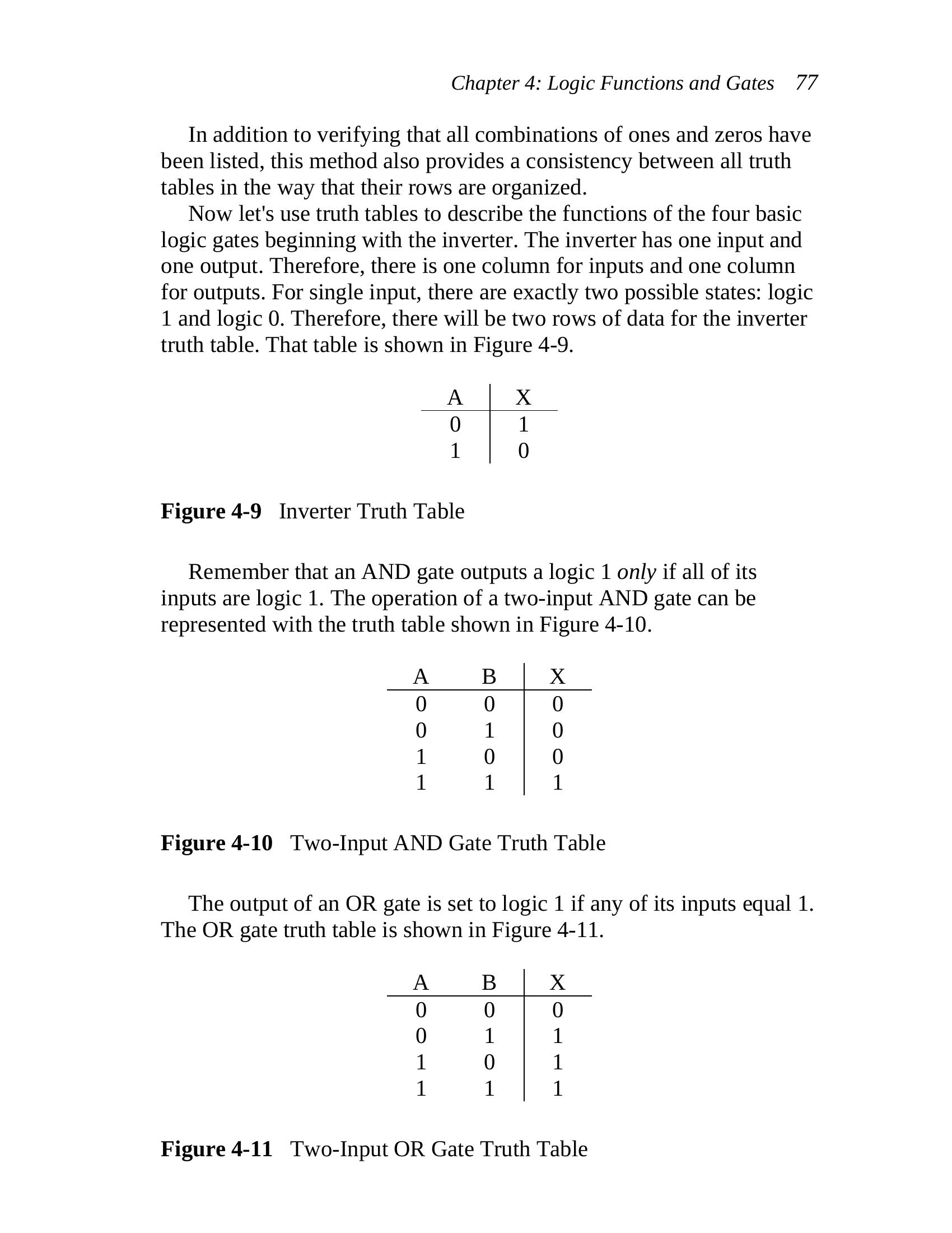
logic gates beginning with the inverter. The inverter has one input and
one output. Therefore, there is one column for inputs and one column
for outputs. For single input, there are exactly two possible states: logic
1 and logic 0. Therefore, there will be two rows of data for the inverter
truth table. That table is shown in Figure 4-9.
A X
0 1
1 0
Figure 4-9 Inverter Truth Table
Remember that an AND gate outputs a logic 1 only if all of its
inputs are logic 1. The operation of a two-input AND gate can be
represented with the truth table shown in Figure 4-10.
A B X
0 0 0
0 1 0
1 0 0
1 1 1
Figure 4-10 Two-Input AND Gate Truth Table
The output of an OR gate is set to logic 1 if any of its inputs equal 1.
The OR gate truth table is shown in Figure 4-11.
A B X
0 0 0
0 1 1
1 0 1
1 1 1
Figure 4-11 Two-Input OR Gate Truth Table
78 Computer Organization and Design Fundamentals
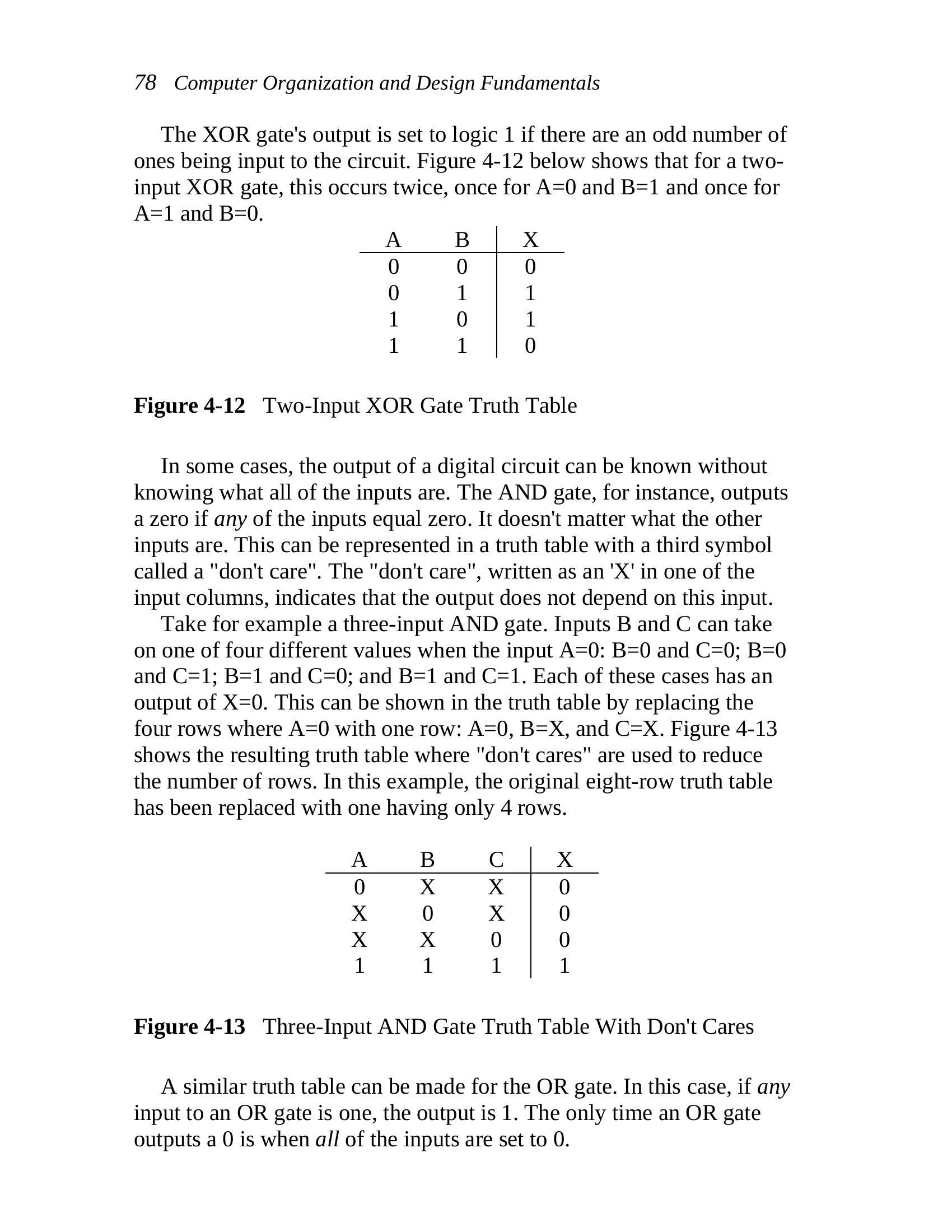
The XOR gate’s output is set to logic 1 if there are an odd number of
ones being input to the circuit. Figure 4-12 below shows that for a two-
input XOR gate, this occurs twice, once for A=0 and B=1 and once for
A=1 and B=0.
A B X
0 0 0
0 1 1
1 0 1
1 1 0
Figure 4-12 Two-Input XOR Gate Truth Table
In some cases, the output of a digital circuit can be known without
knowing what all of the inputs are. The AND gate, for instance, outputs
a zero if any of the inputs equal zero. It doesn’t matter what the other
inputs are. This can be represented in a truth table with a third symbol
called a “don’t care”. The “don’t care”, written as an ‘X’ in one of the
input columns, indicates that the output does not depend on this input.
Take for example a three-input AND gate. Inputs B and C can take
on one of four different values when the input A=0: B=0 and C=0; B=0
and C=1; B=1 and C=0; and B=1 and C=1. Each of these cases has an
output of X=0. This can be shown in the truth table by replacing the
four rows where A=0 with one row: A=0, B=X, and C=X. Figure 4-13
shows the resulting truth table where “don’t cares” are used to reduce
the number of rows. In this example, the original eight-row truth table
has been replaced with one having only 4 rows.
A B C X
0 X X 0
X 0 X 0
X X 0 0
1 1 1 1
Figure 4-13 Three-Input AND Gate Truth Table With Don’t Cares
A similar truth table can be made for the OR gate. In this case, if any
input to an OR gate is one, the output is 1. The only time an OR gate
outputs a 0 is when all of the inputs are set to 0.
Chapter 4: Logic Functions and Gates 79
4.3 Timing Diagrams for Gates
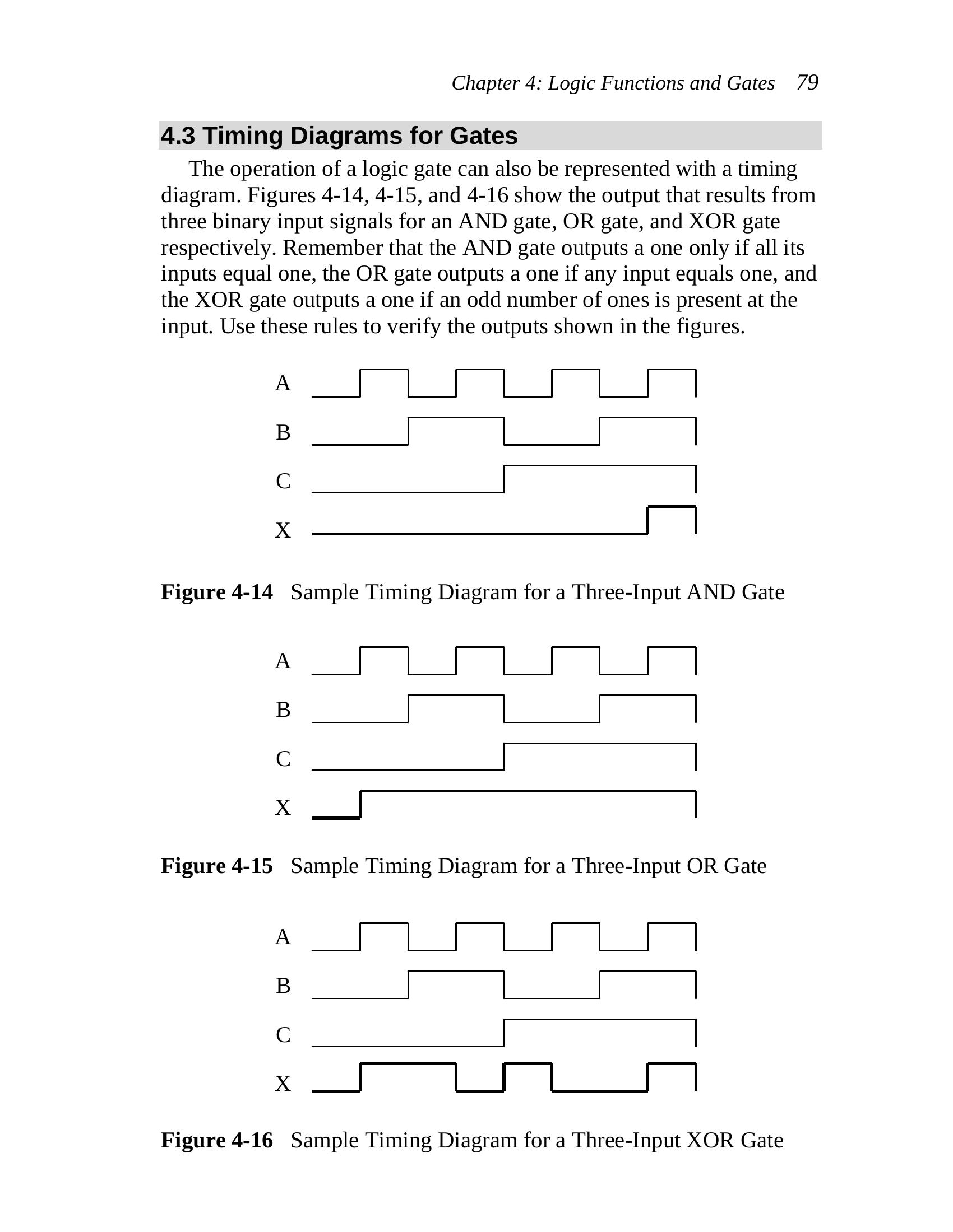
The operation of a logic gate can also be represented with a timing
diagram. Figures 4-14, 4-15, and 4-16 show the output that results from
three binary input signals for an AND gate, OR gate, and XOR gate
respectively. Remember that the AND gate outputs a one only if all its
inputs equal one, the OR gate outputs a one if any input equals one, and
the XOR gate outputs a one if an odd number of ones is present at the
input. Use these rules to verify the outputs shown in the figures.
A
B
C
X
Figure 4-14 Sample Timing Diagram for a Three-Input AND Gate
A
B
C
X
Figure 4-15 Sample Timing Diagram for a Three-Input OR Gate
A
B
C
X
Figure 4-16 Sample Timing Diagram for a Three-Input XOR Gate
80 Computer Organization and Design Fundamentals
4.4 Combinational Logic
By themselves, logic gates are not very practical. Their power
comes when you combine them to create combinational logic.
Combinational logic connects multiple logic gates by using the outputs
from some of the gates as the inputs to others. Figure 4-17 presents a
sample of combinational logic.
A
B X
C
Figure 4-17 Sample Combinational Logic
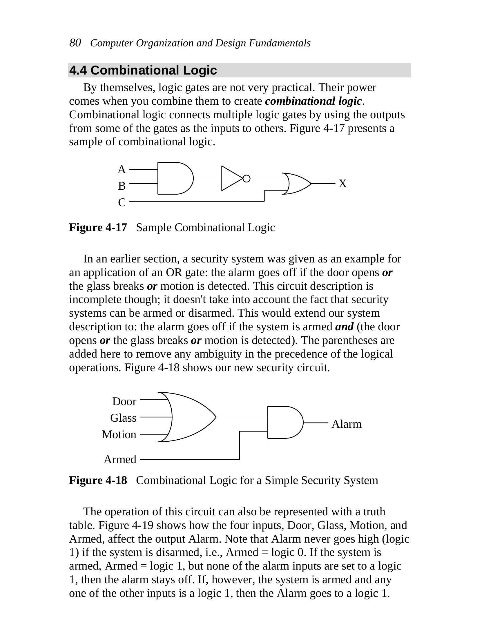
In an earlier section, a security system was given as an example for
an application of an OR gate: the alarm goes off if the door opens or
the glass breaks or motion is detected. This circuit description is
incomplete though; it doesn’t take into account the fact that security
systems can be armed or disarmed. This would extend our system
description to: the alarm goes off if the system is armed and (the door
opens or the glass breaks or motion is detected). The parentheses are
added here to remove any ambiguity in the precedence of the logical
operations. Figure 4-18 shows our new security circuit.
Door
Glass
Alarm
Motion
Armed
Figure 4-18 Combinational Logic for a Simple Security System
The operation of this circuit can also be represented with a truth
table. Figure 4-19 shows how the four inputs, Door, Glass, Motion, and
Armed, affect the output Alarm. Note that Alarm never goes high (logic
1) if the system is disarmed, i.e., Armed = logic 0. If the system is
armed, Armed = logic 1, but none of the alarm inputs are set to a logic
1, then the alarm stays off. If, however, the system is armed and any
one of the other inputs is a logic 1, then the Alarm goes to a logic 1.
Chapter 4: Logic Functions and Gates 81
Armed Door Glass Motion Alarm
0 0 0 0 0
0 0 0 1 0
0 0 1 0 0
0 0 1 1 0
0 1 0 0 0
0 1 0 1 0
0 1 1 0 0
0 1 1 1 0
1 0 0 0 0
1 0 0 1 1
1 0 1 0 1
1 0 1 1 1
1 1 0 0 1
1 1 0 1 1
1 1 1 0 1
1 1 1 1 1
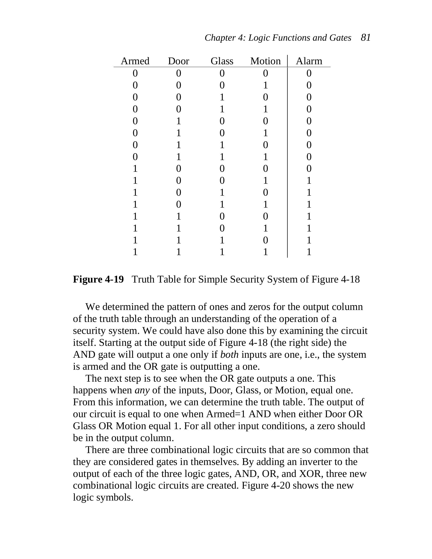
Figure 4-19 Truth Table for Simple Security System of Figure 4-18
We determined the pattern of ones and zeros for the output column
of the truth table through an understanding of the operation of a
security system. We could have also done this by examining the circuit
itself. Starting at the output side of Figure 4-18 (the right side) the
AND gate will output a one only if both inputs are one, i.e., the system
is armed and the OR gate is outputting a one.
The next step is to see when the OR gate outputs a one. This
happens when any of the inputs, Door, Glass, or Motion, equal one.
From this information, we can determine the truth table. The output of
our circuit is equal to one when Armed=1 AND when either Door OR
Glass OR Motion equal 1. For all other input conditions, a zero should
be in the output column.
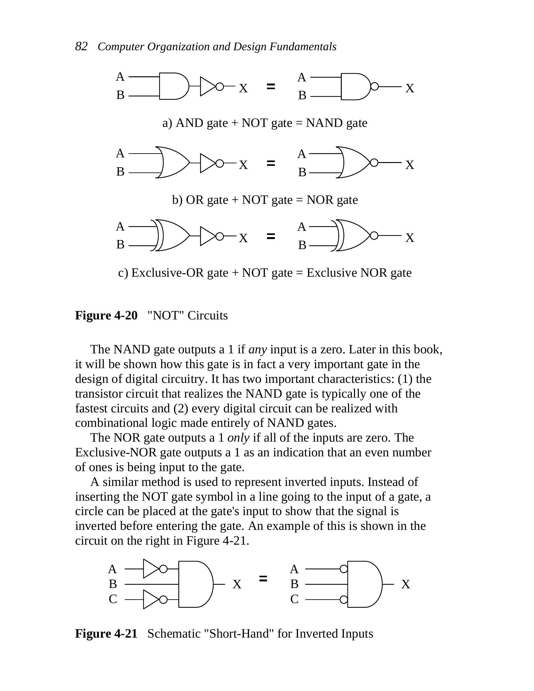
There are three combinational logic circuits that are so common that
they are considered gates in themselves. By adding an inverter to the
output of each of the three logic gates, AND, OR, and XOR, three new
combinational logic circuits are created. Figure 4-20 shows the new
logic symbols.
82 Computer Organization and Design Fundamentals
A A
X X
B B
a) AND gate + NOT gate = NAND gate
A A
X X
B B
b) OR gate + NOT gate = NOR gate
A A
X X
B B
c) Exclusive-OR gate + NOT gate = Exclusive NOR gate
Figure 4-20 “NOT” Circuits
The NAND gate outputs a 1 if any input is a zero. Later in this book,
it will be shown how this gate is in fact a very important gate in the
design of digital circuitry. It has two important characteristics: (1) the
transistor circuit that realizes the NAND gate is typically one of the
fastest circuits and (2) every digital circuit can be realized with
combinational logic made entirely of NAND gates.
The NOR gate outputs a 1 only if all of the inputs are zero. The
Exclusive-NOR gate outputs a 1 as an indication that an even number
of ones is being input to the gate.
A similar method is used to represent inverted inputs. Instead of
inserting the NOT gate symbol in a line going to the input of a gate, a
circle can be placed at the gate’s input to show that the signal is
inverted before entering the gate. An example of this is shown in the
circuit on the right in Figure 4-21.
A A
B X B X
C C
Figure 4-21 Schematic “Short-Hand” for Inverted Inputs
Chapter 4: Logic Functions and Gates 83
4.5 Truth Tables for Combinational Logic
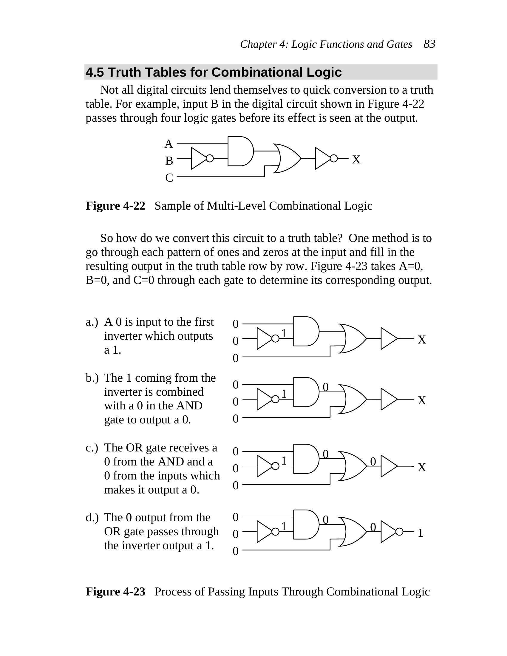
Not all digital circuits lend themselves to quick conversion to a truth
table. For example, input B in the digital circuit shown in Figure 4-22
passes through four logic gates before its effect is seen at the output.
A
B X
C
Figure 4-22 Sample of Multi-Level Combinational Logic
So how do we convert this circuit to a truth table? One method is to
go through each pattern of ones and zeros at the input and fill in the
resulting output in the truth table row by row. Figure 4-23 takes A=0,
B=0, and C=0 through each gate to determine its corresponding output.
a.) A 0 is input to the first 0
1
inverter which outputs
0 X
a 1.
0
b.) The 1 coming from the
0
0
inverter is combined 1
0 X
with a 0 in the AND
gate to output a 0. 0
c.) The OR gate receives a
0
0
0 from the AND and a 1 0
0 X
0 from the inputs which
0
makes it output a 0.
d.) The 0 output from the 0 0
1 0
OR gate passes through 0 1
the inverter output a 1.
0
Figure 4-23 Process of Passing Inputs Through Combinational Logic
84 Computer Organization and Design Fundamentals
This process can be rather tedious, especially if there are more than
three inputs to the combinational logic. Note that the bit pattern in
Figure 4-23 represents only one row of a truth table with eight rows.
Add another input and the truth table doubles in size to sixteen rows.
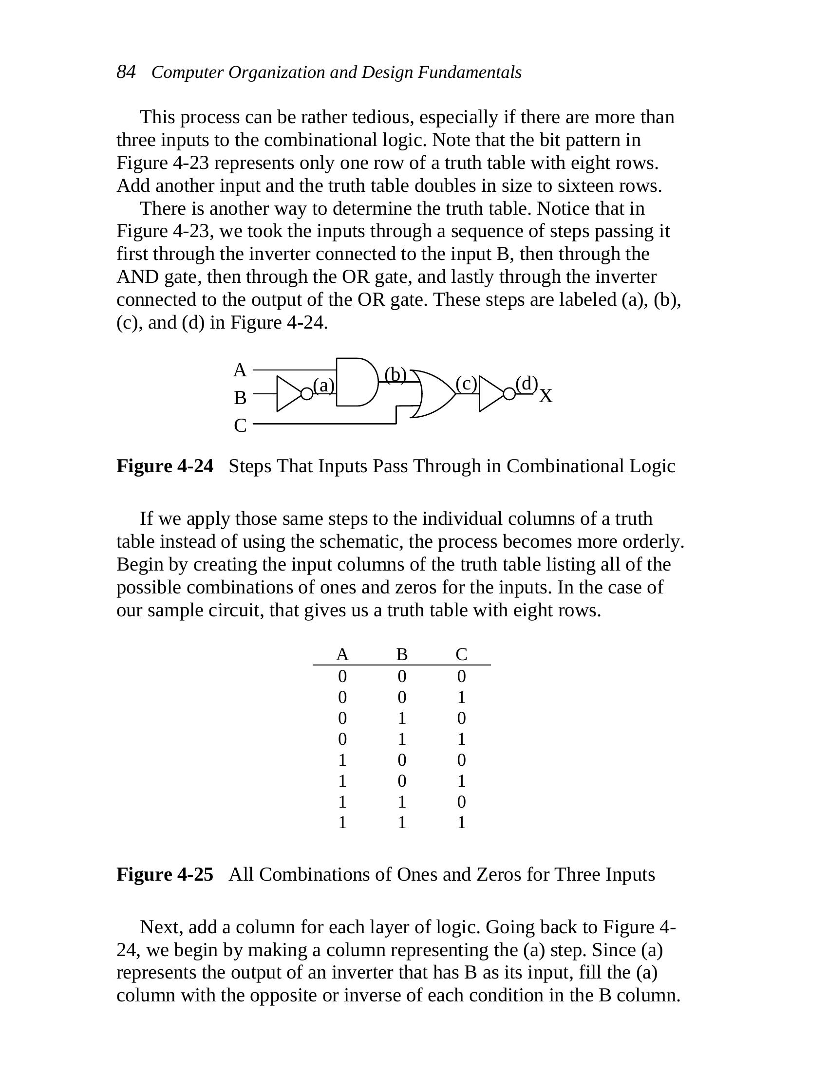
There is another way to determine the truth table. Notice that in
Figure 4-23, we took the inputs through a sequence of steps passing it
first through the inverter connected to the input B, then through the
AND gate, then through the OR gate, and lastly through the inverter
connected to the output of the OR gate. These steps are labeled (a), (b),
(c), and (d) in Figure 4-24.
A
(b)
(a) (c) (d)
B X
C
Figure 4-24 Steps That Inputs Pass Through in Combinational Logic
If we apply those same steps to the individual columns of a truth
table instead of using the schematic, the process becomes more orderly.
Begin by creating the input columns of the truth table listing all of the
possible combinations of ones and zeros for the inputs. In the case of
our sample circuit, that gives us a truth table with eight rows.
A B C
0 0 0
0 0 1
0 1 0
0 1 1
1 0 0
1 0 1
1 1 0
1 1 1
Figure 4-25 All Combinations of Ones and Zeros for Three Inputs
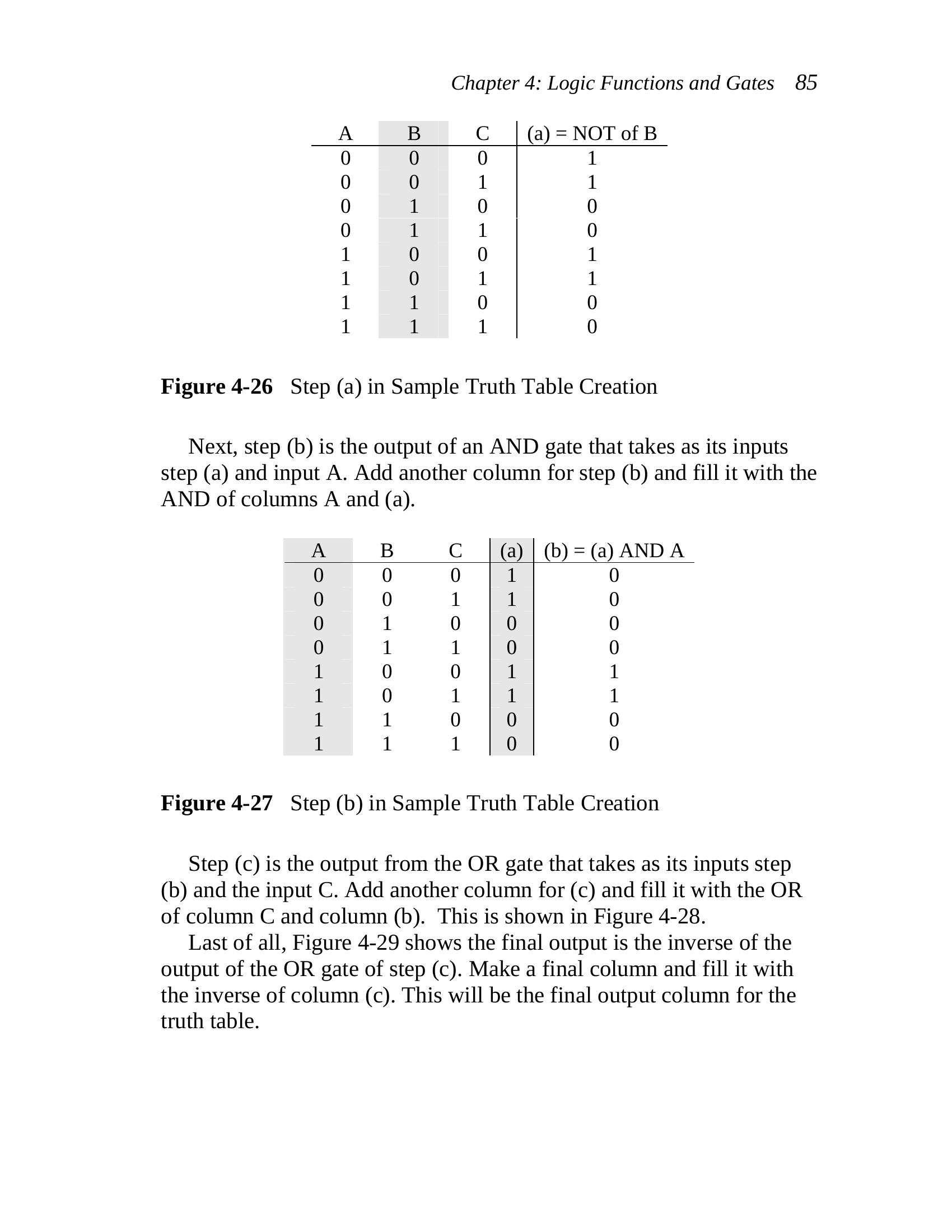
Next, add a column for each layer of logic. Going back to Figure 4-
24, we begin by making a column representing the (a) step. Since (a)
represents the output of an inverter that has B as its input, fill the (a)
column with the opposite or inverse of each condition in the B column.
Chapter 4: Logic Functions and Gates 85
A B C (a) = NOT of B
0 0 0 1
0 0 1 1
0 1 0 0
0 1 1 0
1 0 0 1
1 0 1 1
1 1 0 0
1 1 1 0
Figure 4-26 Step (a) in Sample Truth Table Creation
Next, step (b) is the output of an AND gate that takes as its inputs
step (a) and input A. Add another column for step (b) and fill it with the
AND of columns A and (a).
A B C (a) (b) = (a) AND A
0 0 0 1 0
0 0 1 1 0
0 1 0 0 0
0 1 1 0 0
1 0 0 1 1
1 0 1 1 1
1 1 0 0 0
1 1 1 0 0
Figure 4-27 Step (b) in Sample Truth Table Creation
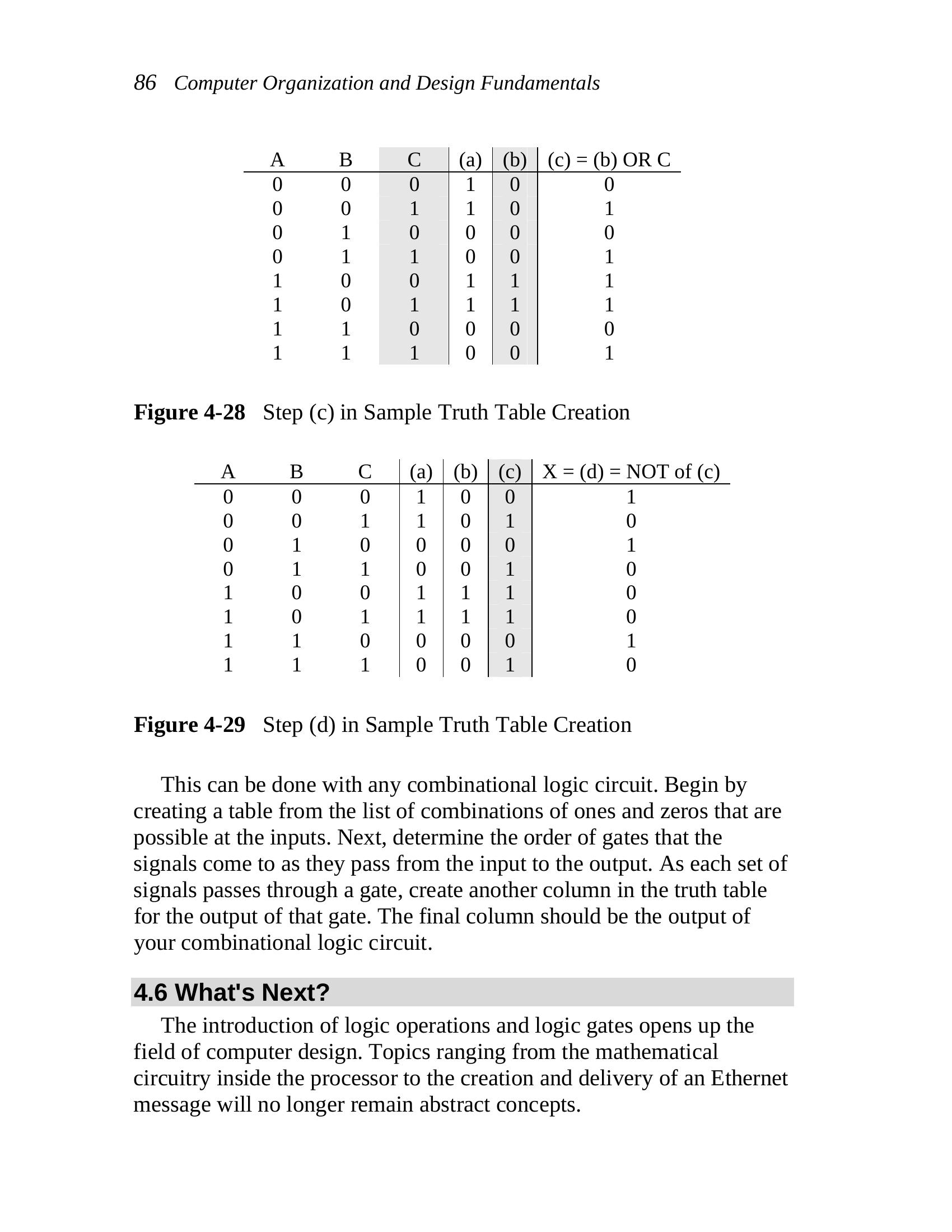
Step (c) is the output from the OR gate that takes as its inputs step
(b) and the input C. Add another column for (c) and fill it with the OR
of column C and column (b). This is shown in Figure 4-28.
Last of all, Figure 4-29 shows the final output is the inverse of the
output of the OR gate of step (c). Make a final column and fill it with
the inverse of column (c). This will be the final output column for the
truth table.
| B | ||
| 0 | ||
| 0 | ||
| 1 | ||
| 1 | ||
| 0 | ||
| 0 | ||
| 1 | ||
| 1 |
| A | ||
| 0 | ||
| 0 | ||
| 0 | ||
| 0 | ||
| 1 | ||
| 1 | ||
| 1 | ||
| 1 |
| (a) | ||
| 1 | ||
| 1 | ||
| 0 | ||
| 0 | ||
| 1 | ||
| 1 | ||
| 0 | ||
| 0 |
86 Computer Organization and Design Fundamentals
A B C (a) (b) (c) = (b) OR C
0 0 0 1 0 0
0 0 1 1 0 1
0 1 0 0 0 0
0 1 1 0 0 1
1 0 0 1 1 1
1 0 1 1 1 1
1 1 0 0 0 0
1 1 1 0 0 1
Figure 4-28 Step (c) in Sample Truth Table Creation
A B C (a) (b) (c) X = (d) = NOT of (c)
0 0 0 1 0 0 1
0 0 1 1 0 1 0
0 1 0 0 0 0 1
0 1 1 0 0 1 0
1 0 0 1 1 1 0
1 0 1 1 1 1 0
1 1 0 0 0 0 1
1 1 1 0 0 1 0
Figure 4-29 Step (d) in Sample Truth Table Creation
This can be done with any combinational logic circuit. Begin by
creating a table from the list of combinations of ones and zeros that are
possible at the inputs. Next, determine the order of gates that the
signals come to as they pass from the input to the output. As each set of
signals passes through a gate, create another column in the truth table
for the output of that gate. The final column should be the output of
your combinational logic circuit.
4.6 What’s Next?
The introduction of logic operations and logic gates opens up the
field of computer design. Topics ranging from the mathematical
circuitry inside the processor to the creation and delivery of an Ethernet
message will no longer remain abstract concepts.
| C | |
| 0 | |
| 1 | |
| 0 | |
| 1 | |
| 0 | |
| 1 | |
| 0 | |
| 1 |
| (b) | |
| 0 | |
| 0 | |
| 0 | |
| 0 | |
| 1 | |
| 1 | |
| 0 | |
| 0 |
| (c) | ||
| 0 | ||
| 1 | ||
| 0 | ||
| 1 | ||
| 1 | ||
| 1 | ||
| 0 | ||
| 1 |
Chapter 4: Logic Functions and Gates 87
Chapter 5 presents a mathematical-like method for representing
logic circuits along with some techniques to manipulate them for faster
performance or a lower chip count. These tools can then be used to
effectively design the components of a computer system.
Problems
1. Identify a real-world example for an AND gate and one for an OR
gate other than those presented in this chapter.
2. How many rows does the truth table for a 4-input logic gate have?
3. Construct the truth table for a four-input OR gate.
4. Construct the truth table for a two-input NAND gate.
5. Construct the truth table for a three-input Exclusive-NOR gate.
6. Construct the truth table for a three-input OR gate using don’t cares
for the inputs similar to the truth table constructed for the three-
input AND gate shown in Figure 4-13.
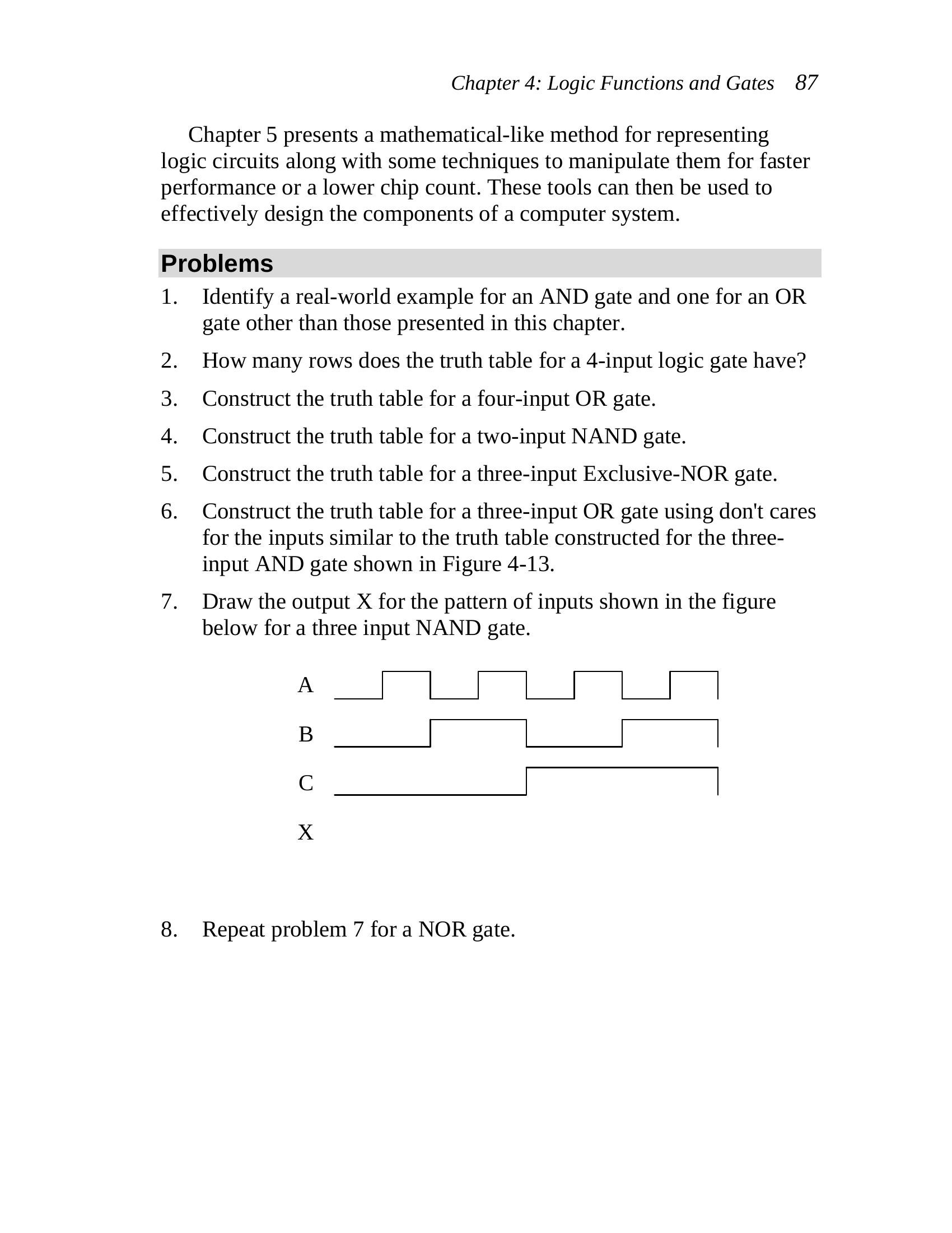
7. Draw the output X for the pattern of inputs shown in the figure
below for a three input NAND gate.
A
B
C
X
8. Repeat problem 7 for a NOR gate.
88 Computer Organization and Design Fundamentals
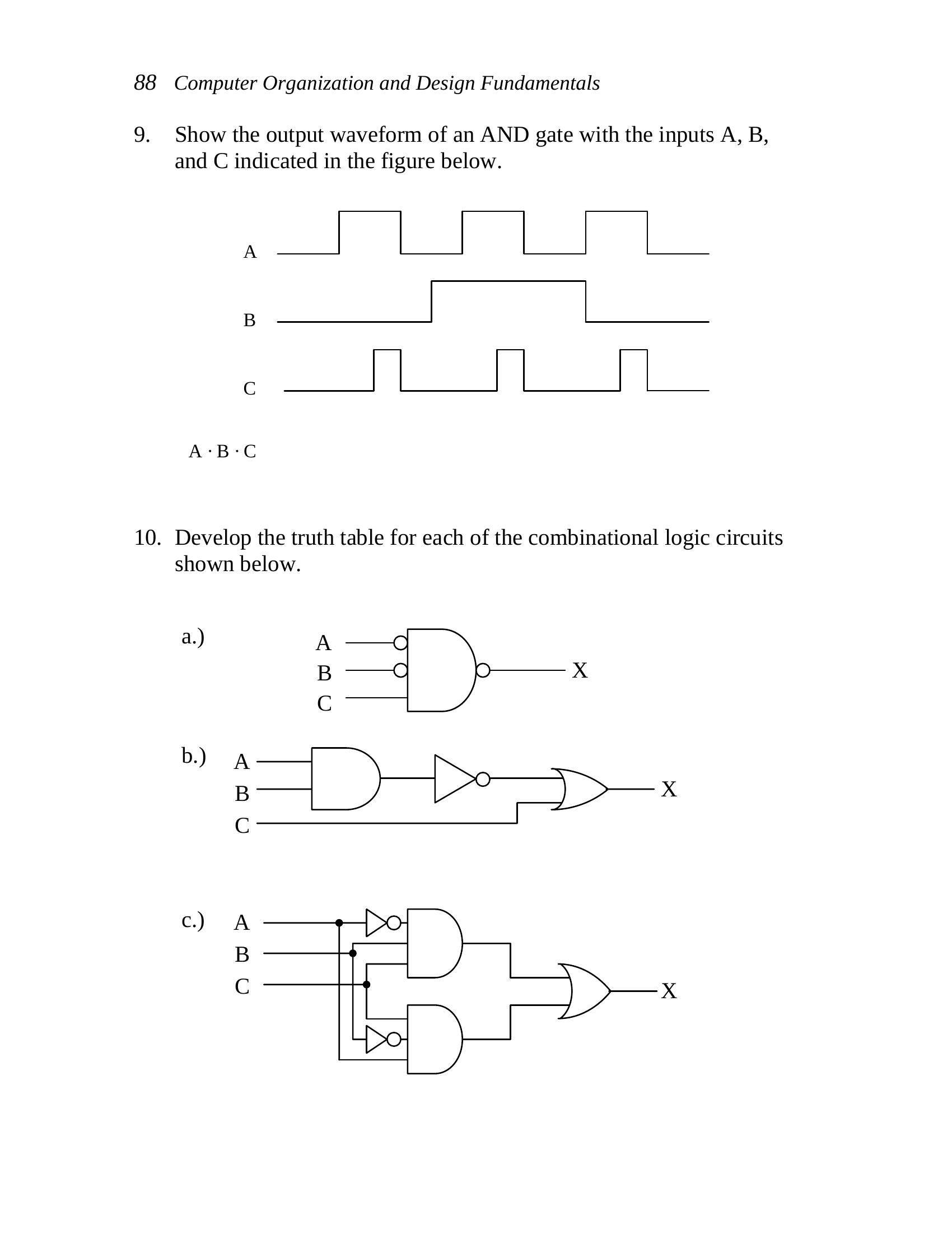
9. Show the output waveform of an AND gate with the inputs A, B,
and C indicated in the figure below.
A
B
C
A · B · C
10. Develop the truth table for each of the combinational logic circuits
shown below.
a.)
A
B X
C
b.)
A
B X
C
c.) A
B
C X
