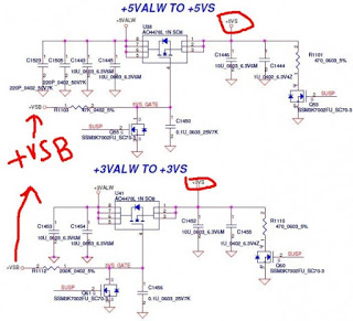
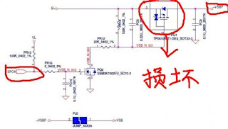
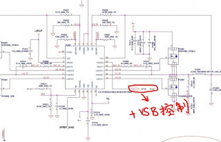
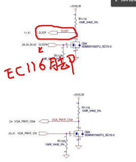
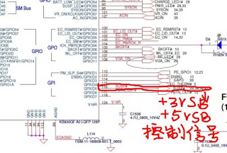
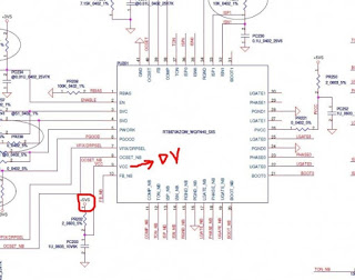
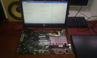
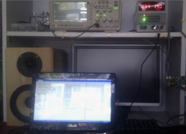
| 1 e0 | * the p5 x + i ” 5 L, ‘of O2 t -! a) & O a $ P ‘m,, P3, k-) e – e3 ~~ / G (? 6 Q: b! r + e, _! U-) l The-A, $ g (S * of F0 the G “K # which the W * of ZN! R5 | ‘[8 g9 S2, x : `+ p9 _4? for 5 s 0 S-; l The * Q-) T-& O6 X- today to take over a peer sent the ASUS the X43B notebook, brought the board been ripped out, almost all new this with about two months or so, because of the local ASUS sale, and so sent to the computer repair shop. Fee if less, the point at turn I peer said a few seconds of power on power-down, the first impression is the voltage on the board did not come out, so the board on the regulator power to take down, and sure enough on the electric current ran 0.13 about power-down and began measuring the major inductance voltage electricity, being able to standby voltage should be normal, by the measured inductance (PL303) +3 VALW (PL305) +5 VALW standby voltage is normal (PL401) 1.8V, 1.05V, (PL701 ) 1.12V, (PL501) 1.5V, (PL901) 0.9 normal, and measured (PL202) no voltage, normally 0.9V (PL204) CPU power supply without voltage, normally 1.1V, the CPU power supply did not come out, the problem where download a copy of this board (X43BLA-7321PR10) drawings, find high-end CPUDC-DC circuit pipe PQ202 PQ206 voltage 19V normal, CPUDC-DC power supply IC is RT8870A APU-CORE output first measured in this forum its power supply VCC, 9 feet, no voltage, normal 5V voltage (PDF labeled +5 the VS), check schematic +5 VS converted from (U38) from +5 VALW standby voltage measured U38 D very 5V, S also no voltage to output voltage measured gets +3 VS analysis should be two public control circuit, the first test (U38) G, pole voltage, and then along the G pole down to view drawings and a small the Q55D FET pole connected to D is very a + VSB voltage the +3 VSG very connected with the Q61D same Q61D pole by a resistor connected to the + VSB. Normal do not know how much I do not know the normal value is how much emphasis and control signals to thought control circuit problem, so there is no bother about it, and then they began to check Q55G control signal SUSP 5V, the signal also controls +3 VS (U41) voltage. Look at the drawings of this signal the for EC116 foot control output, measured in the two states of the standby and power 3.3V jump and combination on electricity, other circuits have a voltage output, so little possibility of damage by the EC chips, EC damage is unlikely to control the signal is also normal to issue, no output, while watching the drawing and watching the board back to think about that + VSB is also analyzed the circuit this voltage, otherwise it is impossible to control on a very MOS transistor after the analysis, maintenance ideas focus on the check the voltage of + VSB find this drawing 35 + VSB is schematic voltage by two FET (PQ1, PQ2) converted from the first measured the PQ1 three feet voltage 1 foot 0V voltage, 3 feet 18.9V, 2 feet 18.4V PQ2G very by SPOK signal control by the standby chip RT8205 23 feet issued, measured at 5V normal, PQ1, 1 foot that is, + VSB is the voltage, the circuit control signal to normal input voltage, measured related resistance without exception, immediately the PQ2 replace the power-on still OQ1 still no output, it suspected the PQ1 itself damage the board remove the fee the same channel tube, through the power measured one foot for 18.3V hearts delight, power-on and then measuring the inductance PL202, PL204 voltage out, 0.9V to, 1.1V board is also no longer power-down, the current soaring, long absence ASUSLOGO out. This board to the maintenance of the end of tomorrow offer, call it a day. I |

