Voltage Regulator Module (VRM)
and Enterprise Voltage
Regulator-Down (EVRD) 10.0
Design Guidelines
July 2005
Document Number: 302731-002
| None | None | |
VRM and EVRD 10.0 Design Guidelines
R
INFORMATION IN THIS DOCUMENT IS PROVIDED IN CONNECTION WITH INTEL® PRODUCTS. NO LICENSE,
EXPRESS OR IMPLIED, BY ESTOPPEL OR OTHERWISE, TO ANY INTELLECTUAL PROPERTY RIGHTS IS GRANTED BY
THIS DOCUMENT. EXCEPT AS PROVIDED IN INTEL’S TERMS AND CONDITIONS OF SALE FOR SUCH PRODUCTS,
INTEL ASSUMES NO LIABILITY WHATSOEVER, AND INTEL DISCLAIMS ANY EXPRESS OR IMPLIED WARRANTY,
RELATING TO SALE AND/OR USE OF INTEL PRODUCTS INCLUDING LIABILITY OR WARRANTIES RELATING TO
FITNESS FOR A PARTICULAR PURPOSE, MERCHANTABILITY, OR INFRINGEMENT OF ANY PATENT, COPYRIGHT OR
OTHER INTELLECTUAL PROPERTY RIGHT. Intel products are not intended for use in medical, life saving, or life sustaining
applications.
Intel may make changes to specifications and product descriptions at any time, without notice.
Designers must not rely on the absence or characteristics of any features or instructions marked “reserved” or “undefined.”
Intel reserves these for future definition and shall have no responsibility whatsoever for conflicts or incompatibilities arising
from future changes to them.
Intel processors may contain design defects or errors known as errata that may cause the product to deviate from published
specifications. Current characterized errata are available on request.
Intel, Intel Xeon, Pentium and the Intel logo are trademarks or registered trademarks of Intel Corporation or its subsidiaries in
the United States and other countries.
∆
Intel processor numbers are not a measure of performance. Processor numbers differentiate features within each processor
family, not across different processor families. See www.intel.com/products/processor_number for details.
* Other names and brands may be claimed as the property of others.
Copyright © 2005 Intel Corporation
2
| None | |
| None | |
VRM and EVRD 10.0 Design Guidelines
R
Contents
1 Applications…………………………………………………………………………………………………8
1.1 Terminology……………………………………………………………………………………..8
2 Output Voltage Requirements………………………………………………………………………10
2.1 Voltage and Current REQUIRED………………………………………………………10
2.2 Load Line Definitions REQUIRED…………………………………………………….12
2.3 Voltage Tolerance REQUIRED…………………………………………………………13
2.4 Processor Vcc Overshoot REQUIRED………………………………………………13
2.5 Stability REQUIRED………………………………………………………………………..14
2.6 Processor Power Sequencing REQUIRED………………………………………..14
2.7 Dynamic Voltage Identification (VID) REQUIRED……………………………….15
2.8 Overshoot at Turn-On or Turn-Off REQUIRED…………………………………..16
2.9 Output Filter Capacitance REQUIRED………………………………………………16
2.10 Shut-Down Response REQUIRED……………………………………………………17
3 Control Signals…………………………………………………………………………………………..18
3.1 Output Enable (OUTEN) REQUIRED………………………………………………..18
3.2 Voltage Identification (VID[5:0]) REQUIRED………………………………………18
3.3 Differential Remote Sense (VO_SEN+/–) REQUIRED…………………………20
3.4 VRM Present (VRM_pres#) EXPECTED……………………………………………20
4 Input Voltage and Current……………………………………………………………………………22
4.1 Input Voltages EXPECTED………………………………………………………………22
4.2 Load Transient Effects on Input Current EXPECTED………………………….22
5 Processor Voltage Output Protection…………………………………………………………….24
5.1 Over-Voltage Protection (OVP) PROPOSED……………………………………..24
5.2 Over-Current Protection (OCP) PROPOSED……………………………………..24
6 Output Indicators………………………………………………………………………………………..26
6.1 Vcc Power-Good (Vcc_PWRGD) PROPOSED…………………………………..26
6.2 Voltage Regulator Hot (VR_hot#) PROPOSED…………………………………..26
6.3 Load Indicator Output (Load_current) PROPOSED…………………………….27
6.4 VRM Identification (VRM_ID0, VRM_ID1) PROPOSED……………………….27
7 VRM – Mechanical Guidelines……………………………………………………………………..28
7.1 VRM Connector EXPECTED……………………………………………………………28
7.2 VRM Connector Keying……………………………………………………………………28
7.3 Pin Descriptions and Assignments……………………………………………………28
7.4 Mechanical Dimensions PROPOSED………………………………………………..31
7.4.1 Gold Finger Specification…………………………………………………31
8 VRM – Environmental Conditions…………………………………………………………………32
3
| None | |
| None | |
VRM and EVRD 10.0 Design Guidelines
R
8.1 Operating Temperature PROPOSED………………………………………………..32
8.2 VRM Board Temperature REQUIRED……………………………………………….32
8.3 Non-Operating Temperature PROPOSED…………………………………………32
8.4 Humidity PROPOSED……………………………………………………………………..32
8.5 Altitude PROPOSED……………………………………………………………………….32
8.6 Electrostatic Discharge PROPOSED…………………………………………………33
8.7 Shock and Vibration PROPOSED…………………………………………………….33
8.8 Electromagnetic Compatibility PROPOSED……………………………………….33
8.9 Reliability PROPOSED……………………………………………………………………33
8.10 Safety PROPOSED…………………………………………………………………………33
9 Manufacturing Considerations……………………………………………………………………..34
9.1 Lead Free (Pb Free)………………………………………………………………………..34
Figures
Figure 1. VRM/EVRD 10.0 Load Current vs. Time for Intel® Xeon™ Processor with 800
MHz System Bus………………………………………………………………………………………….10
Figure 2 VRM/EVRD 10.0 Load Current vs. Time for Low Voltage Intel® Xeon™
Processor with 800 MHz System Bus……………………………………………………………..11
Figure 3. VRM/EVRD 10.0 Die Load Line……………………………………………………………..12
Figure 4. Vcc Overshoot Example Waveform…………………………………………………………13
Figure 5. Power-On Sequence Block Diagram……………………………………………………….14
Figure 6. Power-On Sequence Timing Diagram……………………………………………………..14
Figure 7. Processor Transition States…………………………………………………………………..15
Figure 8. Example Processor VID Transition States……………………………………………….16
Figure 9. Model of Processor Load……………………………………………………………………….17
Figure 10. VRM 10.0 Module and Connector…………………………………………………………31
Tables
Table 1. Icc Guidelines……………………………………………………………………………………….12
Table 2. Capacitor Recommendations………………………………………………………………….17
Table 3. OUTEN Specifications……………………………………………………………………………18
Table 4. VID Specifications………………………………………………………………………………….18
Table 5. Voltage Identification (VID)……………………………………………………………………..19
Table 6. VRM_pres# Specifications………………………………………………………………………20
Table 7. Vcc_PWRGD Specifications……………………………………………………………………26
Table 8. VR_hot# Specifications…………………………………………………………………………..26
Table 9. VRM 10.0 Connector Vendor and Part Numbers……………………………………….28
Table 10. VRM 10.0 Connector Pin Descriptions……………………………………………………29
Table 11. VRM Pins……………………………………………………………………………………………30
4
| None | |
| None | |
VRM and EVRD 10.0 Design Guidelines
R
5
| None | |
| None | |

VRM and EVRD 10.0 Design Guidelines
R
Revision History
Date Revision Description
June 2004 001 Initial release.
June 2005 002 Added references to Low Voltage Intel® Xeon™ processor
with 800 MHz system bus
6
| None | |
| None | |
| Date | Revision | Description |
| June 2004 | 001 | Initial release. |
| June 2005 | 002 | Added references to Low Voltage Intel® Xeon™ processor with 800 MHz system bus |
VRM and EVRD 10.0 Design Guidelines
R
7
| None | |
| None | |

VRM and EVRD 10.0 Design Guidelines
R
1 Applications
This document defines DC-to-DC converters designed to help meet the power requirements of the
Intel® Xeon™ processor with 800 MHz system bus and Low Voltage Intel® Xeon™ processor
with 800 MHz system bus. The intent of this document is to define the electrical, thermal, and
mechanical specifications for VRM 10.0.
VRM – The Voltage Regulator Module (VRM) designation in this document refers to a voltage
regulator that is plugged into a baseboard where the baseboard is designed to support more than
one processor. VRM output requirements in this document are intended to match the needs of a
set of microprocessors.
EVRD – The Enterprise Voltage Regulator-Down (EVRD) designation in this document refers to
a voltage regulator that is embedded in a baseboard where the baseboard is designed to support
more than one processor. EVRD output requirements in this document are intended to match the
needs of a set of microprocessors. Each implementation of a specific baseboard must meet the
specifications of all processors supported by the baseboard.
The specifications in the respective processors’ datasheet always take precedence over the data
provided in this document.
VRM/EVRD 10.0 incorporates functional changes from prior VRD and VRM guidelines:
• Vcc and Vtt supplies are separate (the Vtt specifications are included in the respective
processors’ datasheet).
• Addition of a continuous load current (ICC (TDC)) to enable cost effective VRM/EVRD
designs (Section 2.1).
• Addition of dynamic VID to change the output voltage during normal operation in response
to an input from the processor (Section 2.7).
• Simplified definition of power-good as a power-up indication (Section 6.1).
• Extended use of the VRM/EVRD disable function to turn off the output in response to an
input from the processor (Section 3.1).
• Specifications added to monitor and react to excessive temperature in the voltage regulator
(VR) (Section 6.2)
1.1 Terminology
A ‘#’ symbol after a signal name refers to an active low signal, indicating a signal is in the
asserted state when driven to a low level. For example, when VRM_pres# is low, it indicates that
a VRM is present in the connector.
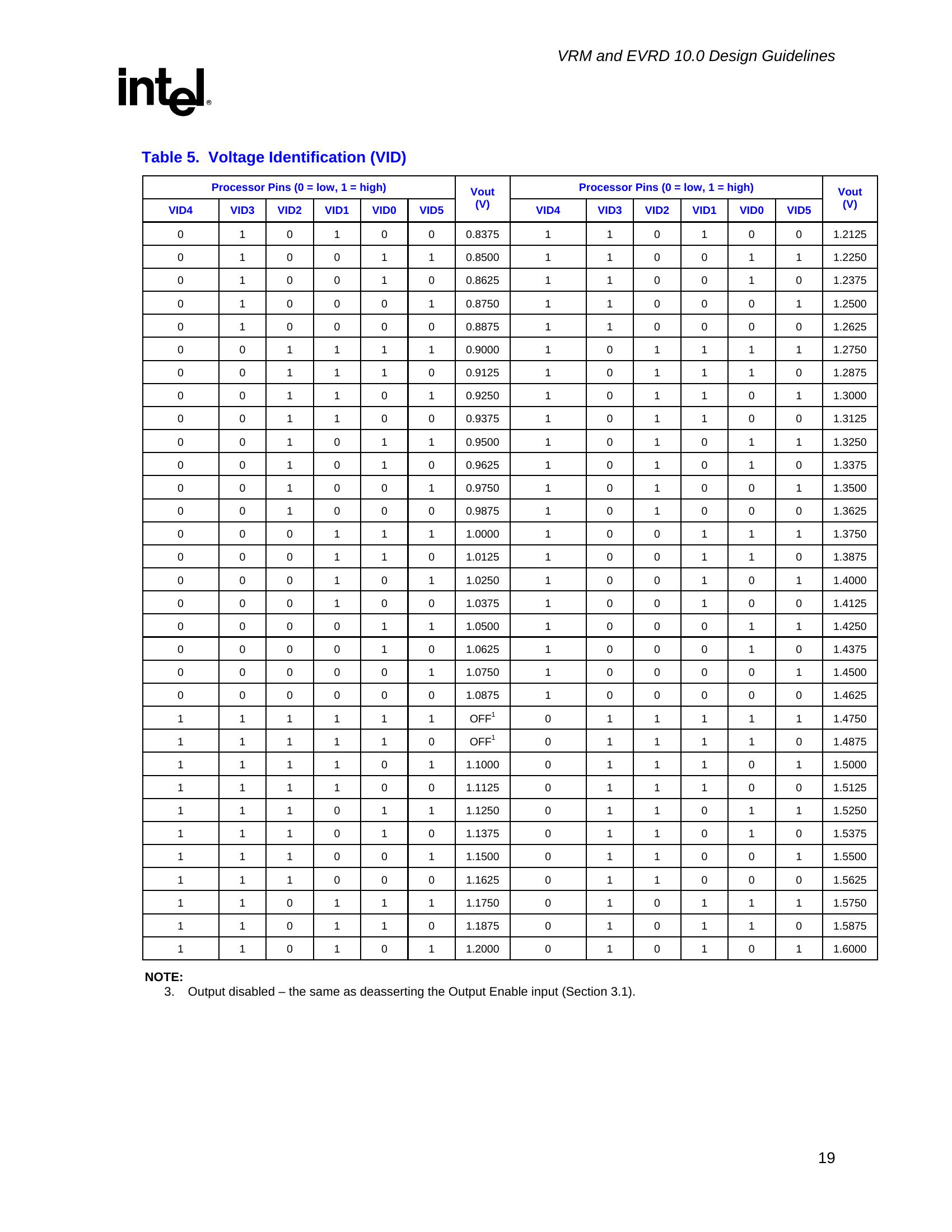
Table 5 specifies the voltage level corresponding to the state of VID[5:0]. A ‘1’ in this table
refers to a high voltage level and a ‘0’ refers to a low voltage level.
8
| None | |
| None | |
VRM and EVRD 10.0 Design Guidelines
R
9
| None | |
| None | |

VRM and EVRD 10.0 Design Guidelines
R
2 Output Voltage Requirements
2.1 Voltage and Current REQUIRED
A 6-bit VID code provided by the processor to the VRM/EVRD determines a reference output
voltage, as described in Section 3.2. Sections 2.2 and 2.3 specify deviations from the VID
reference voltage.
The load lines in Section 2.2 show the relationship between Vcc and Icc for the processor.
For the Intel® Xeon™ processor with 800MHz system bus, the VRM/EVRD will be required to
support the following:
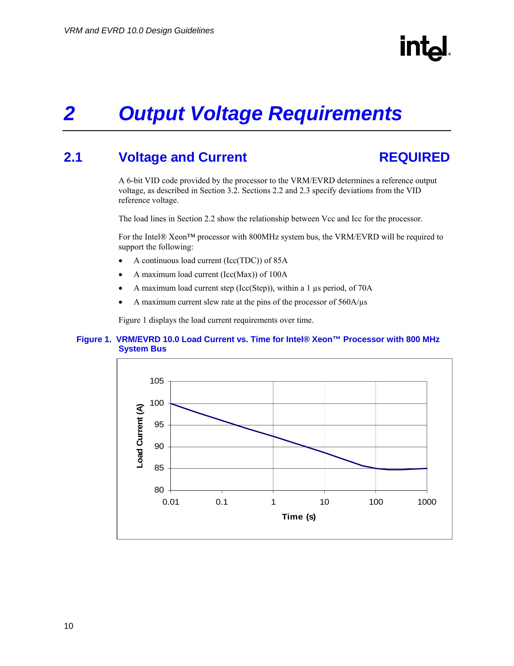
• A continuous load current (Icc(TDC)) of 85A
• A maximum load current (Icc(Max)) of 100A
• A maximum load current step (Icc(Step)), within a 1 µs period, of 70A
• A maximum current slew rate at the pins of the processor of 560A/µs
Figure 1 displays the load current requirements over time.
Figure 1. VRM/EVRD 10.0 Load Current vs. Time for Intel® Xeon™ Processor with 800 MHz
System Bus
105
100
95
90
85
80
0.01 0.1 1 10 100 1000
Time (s)
10
)A(
tnerruC
daoL
| None | |
VRM and EVRD 10.0 Design Guidelines
R
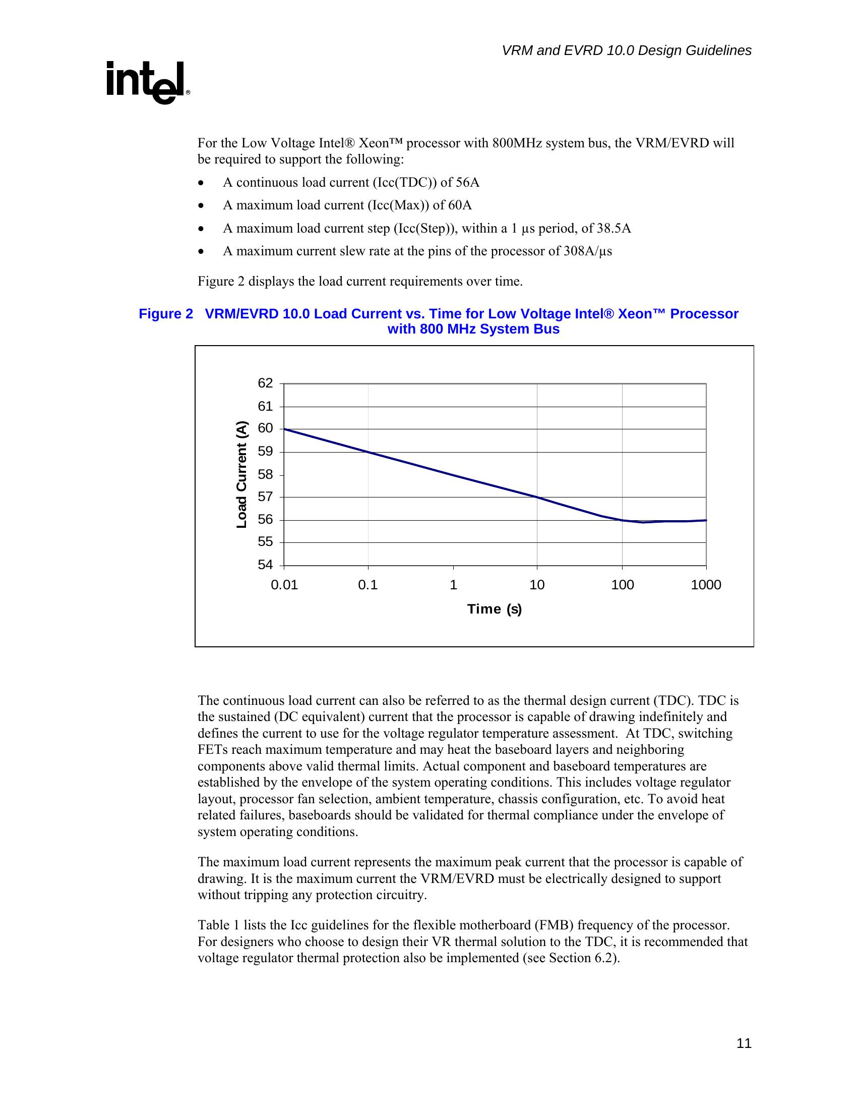
For the Low Voltage Intel® Xeon™ processor with 800MHz system bus, the VRM/EVRD will
be required to support the following:
• A continuous load current (Icc(TDC)) of 56A
• A maximum load current (Icc(Max)) of 60A
• A maximum load current step (Icc(Step)), within a 1 µs period, of 38.5A
• A maximum current slew rate at the pins of the processor of 308A/µs
Figure 2 displays the load current requirements over time.
Figure 2 VRM/EVRD 10.0 Load Current vs. Time for Low Voltage Intel® Xeon™ Processor
with 800 MHz System Bus
62
61
60
59
58
57
56
55
54
0.01 0.1 1 10 100 1000
Time (s)
11
)A(
tnerruC
daoL
The continuous load current can also be referred to as the thermal design current (TDC). TDC is
the sustained (DC equivalent) current that the processor is capable of drawing indefinitely and
defines the current to use for the voltage regulator temperature assessment. At TDC, switching
FETs reach maximum temperature and may heat the baseboard layers and neighboring
components above valid thermal limits. Actual component and baseboard temperatures are
established by the envelope of the system operating conditions. This includes voltage regulator
layout, processor fan selection, ambient temperature, chassis configuration, etc. To avoid heat
related failures, baseboards should be validated for thermal compliance under the envelope of
system operating conditions.
The maximum load current represents the maximum peak current that the processor is capable of
drawing. It is the maximum current the VRM/EVRD must be electrically designed to support
without tripping any protection circuitry.
Table 1 lists the Icc guidelines for the flexible motherboard (FMB) frequency of the processor.
For designers who choose to design their VR thermal solution to the TDC, it is recommended that
voltage regulator thermal protection also be implemented (see Section 6.2).
| None | |
| None | |
VRM and EVRD 10.0 Design Guidelines
R
Table 1. Icc Guidelines
Icc(TDC) (A) Icc(Max) (A) Icc(Step) (A) Slew Rate (A/µs)
Intel® Xeon™ Processor with
85 100 70 560
800 MHz System Bus
Low Voltage Intel® Xeon™
processor with 800 MHz 56 60 38.5 308
system bus
NOTES:
1. See the Intel® Xeon™ Processor with 800 MHz System Bus Datasheet and Low Voltage Intel® Xeon™
processor with 800 MHz System Bus Datasheet for the latest specifications.
2. This table represents the expected operating limitations for VRM/EVRD 10.0. Future Intel® Xeon™
processors with 800 MHz system bus will require a later version of the VRM/EVRD to reach end-of-life
capabilities.
2.2 Load Line Definitions REQUIRED
The following load lines contain static and transient voltage data as well as maximum and
minimum voltage levels. Measurement of the load line is to be done at the remote sense point. It
is required that the remote sense point for the voltage regulator be connected to the processor
VCCSENSE and VSSSENSE pins.
The upper and lower load lines represent the allowable range of voltages that must be presented to
the processor. The voltage must never exceed these boundaries for proper operation of the
processor.
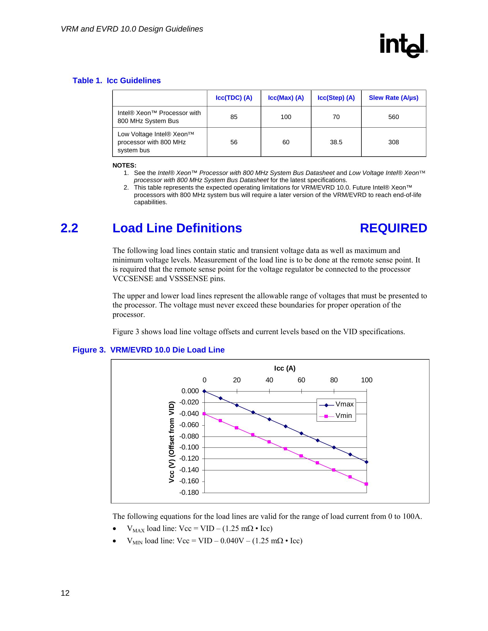
Figure 3 shows load line voltage offsets and current levels based on the VID specifications.
Figure 3. VRM/EVRD 10.0 Die Load Line
Icc (A)
0 20 40 60 80 100
0.000
-0.020
-0.040
-0.060
-0.080
-0.100
-0.120
-0.140
-0.160
-0.180
12
)DIV
morf
tesffO(
)V(
ccV
Vmax
Vmin
The following equations for the load lines are valid for the range of load current from 0 to 100A.
• V load line: Vcc = VID – (1.25 mΩ • Icc)
MAX
• V load line: Vcc = VID – 0.040V – (1.25 mΩ • Icc)
MIN
| None | |
| None | |
| Icc(TDC) (A) | Icc(Max) (A) | Icc(Step) (A) | Slew Rate (A/µs) | |
| Intel® Xeon™ Processor with 800 MHz System Bus | 85 | 100 | 70 | 560 |
| Low Voltage Intel® Xeon™ processor with 800 MHz system bus | 56 | 60 | 38.5 | 308 |
| Icc (A) 0 20 40 60 80 100 0.000 -0.020 )DIV Vmax -0.040 Vmin morf -0.060 -0.080 tesffO( -0.100 -0.120 )V( -0.140 ccV -0.160 -0.180 | ||
| None | None |
| None | None | |
| None | None | |
| Vmax Vmin | ||
| None | None | |
| None | None | |
| None | None | |
| None | None | |
| None | None | |
| None | None | |
| None | None |
VRM and EVRD 10.0 Design Guidelines
R
2.3 Voltage Tolerance REQUIRED
The voltage ranges shown in Section 2.2 include the following tolerances:
• Initial DC output voltage set-point error
• Output ripple and noise
• No-load offset centering error
• Current sensing and droop errors
• Component aging effects
• Full ambient temperature range and warm up
• Dynamic output changes from minimum-to-maximum or maximum-to-minimum load, as
measured over a 20 MHz bandwidth
• Variations of the input voltage
2.4 Processor Vcc Overshoot REQUIRED
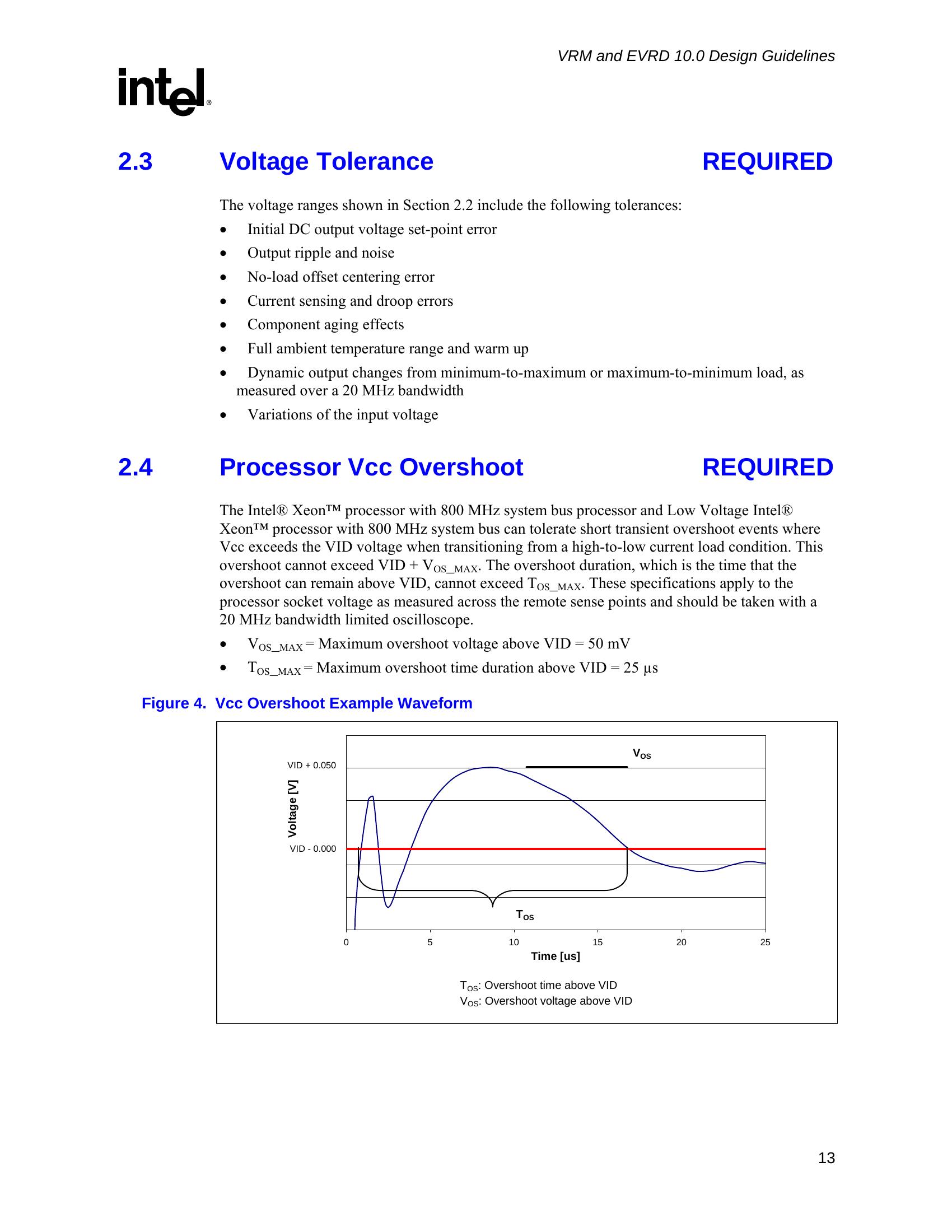
The Intel® Xeon™ processor with 800 MHz system bus processor and Low Voltage Intel®
Xeon™ processor with 800 MHz system bus can tolerate short transient overshoot events where
Vcc exceeds the VID voltage when transitioning from a high-to-low current load condition. This
overshoot cannot exceed VID + V _ . The overshoot duration, which is the time that the
OS MAX
overshoot can remain above VID, cannot exceed T _ . These specifications apply to the
OS MAX
processor socket voltage as measured across the remote sense points and should be taken with a
20 MHz bandwidth limited oscilloscope.
• V _ = Maximum overshoot voltage above VID = 50 mV
OS MAX
• T _ = Maximum overshoot time duration above VID = 25 µs
OS MAX
Figure 4. Vcc Overshoot Example Waveform
0 5 10 15 20 25
Time [us]
13
]V[
egatloV
V
OS
VID + 0.050
VID – 0.000
T
OS
T : Overshoot time above VID
OS
V : Overshoot voltage above VID
OS
| None | |
| None | |
| V OS | None | None |
| None | None | |
| None | None | |
| None | None | |
| None | None | |
| T OS | None | None |
VRM and EVRD 10.0 Design Guidelines
R
2.5 Stability REQUIRED
The VRM/EVRD needs to be unconditionally stable under all specified output voltage ranges and
current transients of any duty cycle and up to repetition rates of 1 MHz. The VRM/EVRD should
be stable under a no load condition.
2.6 Processor Power Sequencing REQUIRED
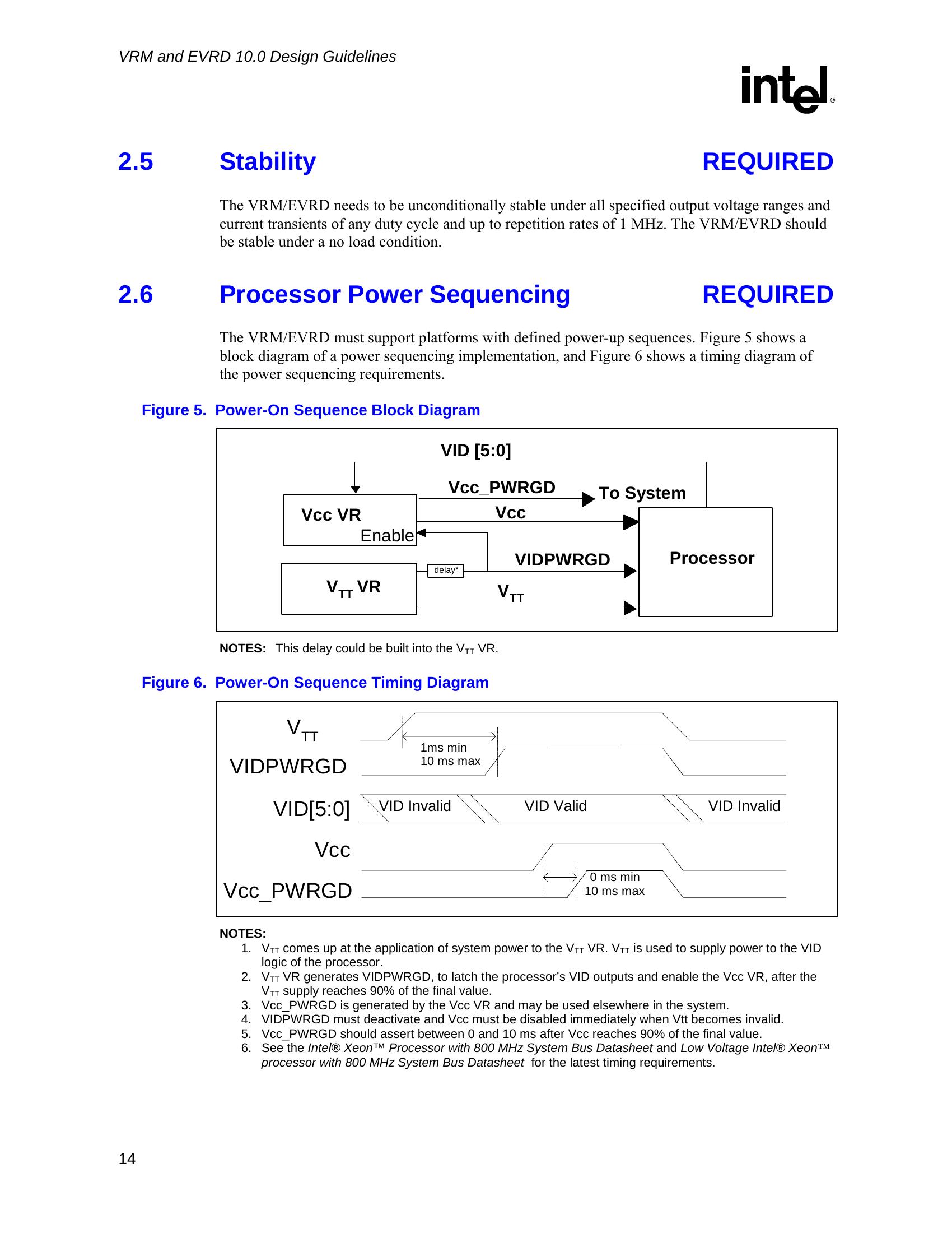
The VRM/EVRD must support platforms with defined power-up sequences. Figure 5 shows a
block diagram of a power sequencing implementation, and Figure 6 shows a timing diagram of
the power sequencing requirements.
Figure 5. Power-On Sequence Block Diagram
VID [5:0]
Vcc_PWRGD
To System
Vcc VR Vcc
Enable
VIDPWRGD Processor
delay*
V VR V
TT TT
NOTES: This delay could be built into the V VR.
TT
Figure 6. Power-On Sequence Timing Diagram
V
TT
1ms min
VIDPWRGD 10 ms max
VID[5:0] VID Invalid VID Valid VID Invalid
Vcc
0 ms min
Vcc_PWRGD 10 ms max
NOTES:
1. V comes up at the application of system power to the V VR. V is used to supply power to the VID
TT TT TT
logic of the processor.
2. V VR generates VIDPWRGD, to latch the processor’s VID outputs and enable the Vcc VR, after the
TT
V supply reaches 90% of the final value.
TT
3. Vcc_PWRGD is generated by the Vcc VR and may be used elsewhere in the system.
4. VIDPWRGD must deactivate and Vcc must be disabled immediately when Vtt becomes invalid.
5. Vcc_PWRGD should assert between 0 and 10 ms after Vcc reaches 90% of the final value.
6. See the Intel® Xeon™ Processor with 800 MHz System Bus Datasheet and Low Voltage Intel® Xeon™
processor with 800 MHz System Bus Datasheet for the latest timing requirements.
14
| None | |
| delay* |
| VID Invalid | VID Valid |
VRM and EVRD 10.0 Design Guidelines
R
2.7 Dynamic Voltage Identification (VID) REQUIRED
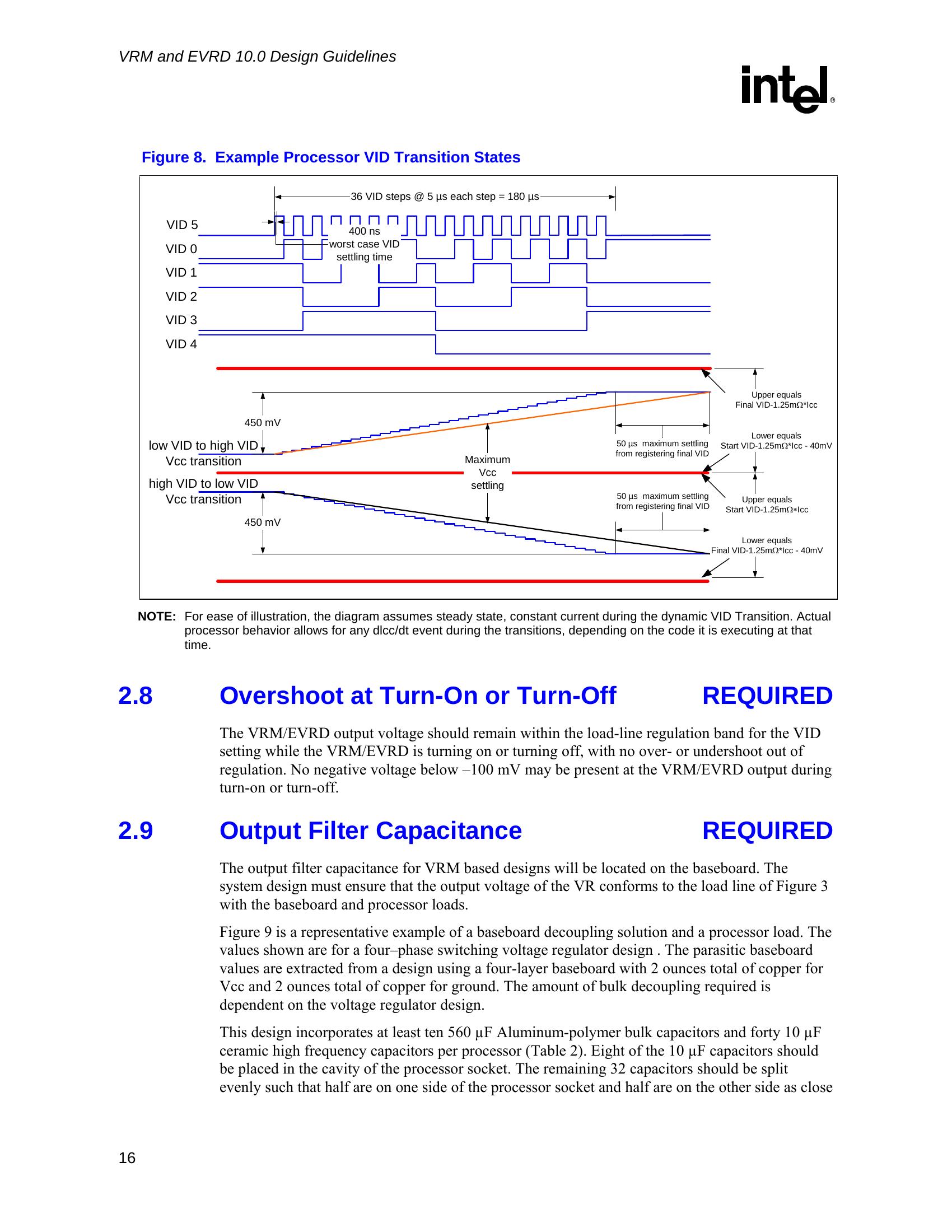
VRM/EVRD 10.0 supports dynamic VID across the entire VID table, which requires the ability to
reduce the load line voltage shown in Figure 3 by 450 mV. The VRM/EVRD must be capable of
accepting voltage level changes of 12.5 mV steps every 5 µs, up to 36 steps (450 mV) in 180 µs.
The low voltage state will be maintained for at least 50 µs. The worst case settling time for the six
VID lines, including line-to-line skew, is 400 ns. The VID inputs should contain circuitry to
prevent false tripping or latching of VID codes during the settling time.
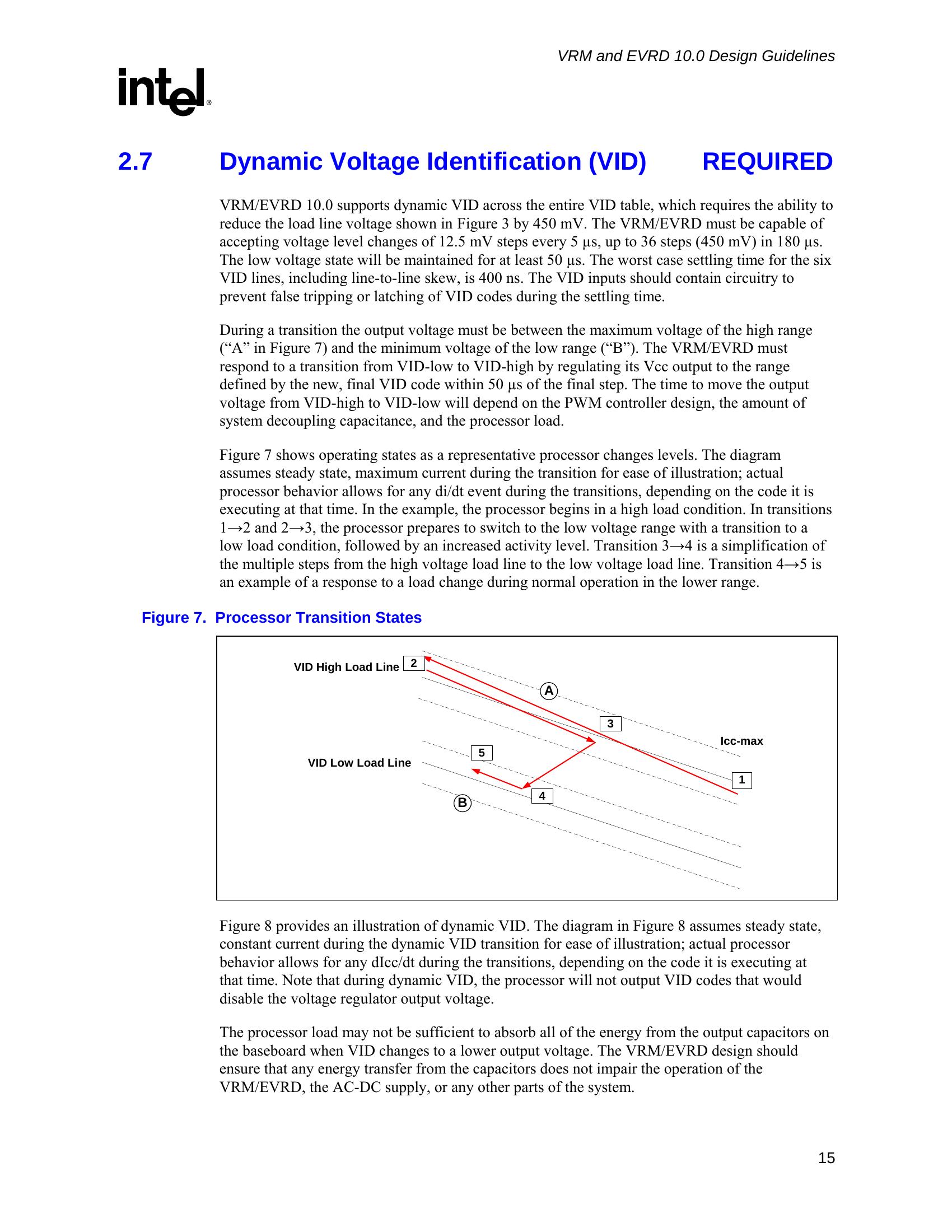
During a transition the output voltage must be between the maximum voltage of the high range
(“A” in Figure 7) and the minimum voltage of the low range (“B”). The VRM/EVRD must
respond to a transition from VID-low to VID-high by regulating its Vcc output to the range
defined by the new, final VID code within 50 µs of the final step. The time to move the output
voltage from VID-high to VID-low will depend on the PWM controller design, the amount of
system decoupling capacitance, and the processor load.
Figure 7 shows operating states as a representative processor changes levels. The diagram
assumes steady state, maximum current during the transition for ease of illustration; actual
processor behavior allows for any di/dt event during the transitions, depending on the code it is
executing at that time. In the example, the processor begins in a high load condition. In transitions
1→2 and 2→3, the processor prepares to switch to the low voltage range with a transition to a
low load condition, followed by an increased activity level. Transition 3→4 is a simplification of
the multiple steps from the high voltage load line to the low voltage load line. Transition 4→5 is
an example of a response to a load change during normal operation in the lower range.
Figure 7. Processor Transition States
VID High Load Line 2
A
3
Icc-max
5
VID Low Load Line
1
4
B
Figure 8 provides an illustration of dynamic VID. The diagram in Figure 8 assumes steady state,
constant current during the dynamic VID transition for ease of illustration; actual processor
behavior allows for any dIcc/dt during the transitions, depending on the code it is executing at
that time. Note that during dynamic VID, the processor will not output VID codes that would
disable the voltage regulator output voltage.
The processor load may not be sufficient to absorb all of the energy from the output capacitors on
the baseboard when VID changes to a lower output voltage. The VRM/EVRD design should
ensure that any energy transfer from the capacitors does not impair the operation of the
VRM/EVRD, the AC-DC supply, or any other parts of the system.
15
| None | |
| None | |
VRM and EVRD 10.0 Design Guidelines
R
Figure 8. Example Processor VID Transition States
36 VID steps @ 5 µs each step = 180 µs
VID 5
400 ns
VID 0 worst case VID
settling time
VID 1
VID 2
VID 3
VID 4
Upper equals
Final VID-1.25mΩ*Icc
450 mV
Lower equals
low VID to high VID 50 µs maximum settling Start VID-1.25mΩ*Icc – 40mV
from registering final VID
Vcc transition Maximum
Vcc
high VID to low VID settling
Vcc transition 50 µs maximum settling Upper equals
from registering final VID Start VID-1.25mΩ∗Icc
450 mV
Lower equals
Final VID-1.25mΩ*Icc – 40mV
NOTE: For ease of illustration, the diagram assumes steady state, constant current during the dynamic VID Transition. Actual
processor behavior allows for any dlcc/dt event during the transitions, depending on the code it is executing at that
time.
2.8 Overshoot at Turn-On or Turn-Off REQUIRED
The VRM/EVRD output voltage should remain within the load-line regulation band for the VID
setting while the VRM/EVRD is turning on or turning off, with no over- or undershoot out of
regulation. No negative voltage below –100 mV may be present at the VRM/EVRD output during
turn-on or turn-off.
2.9 Output Filter Capacitance REQUIRED
The output filter capacitance for VRM based designs will be located on the baseboard. The
system design must ensure that the output voltage of the VR conforms to the load line of Figure 3
with the baseboard and processor loads.
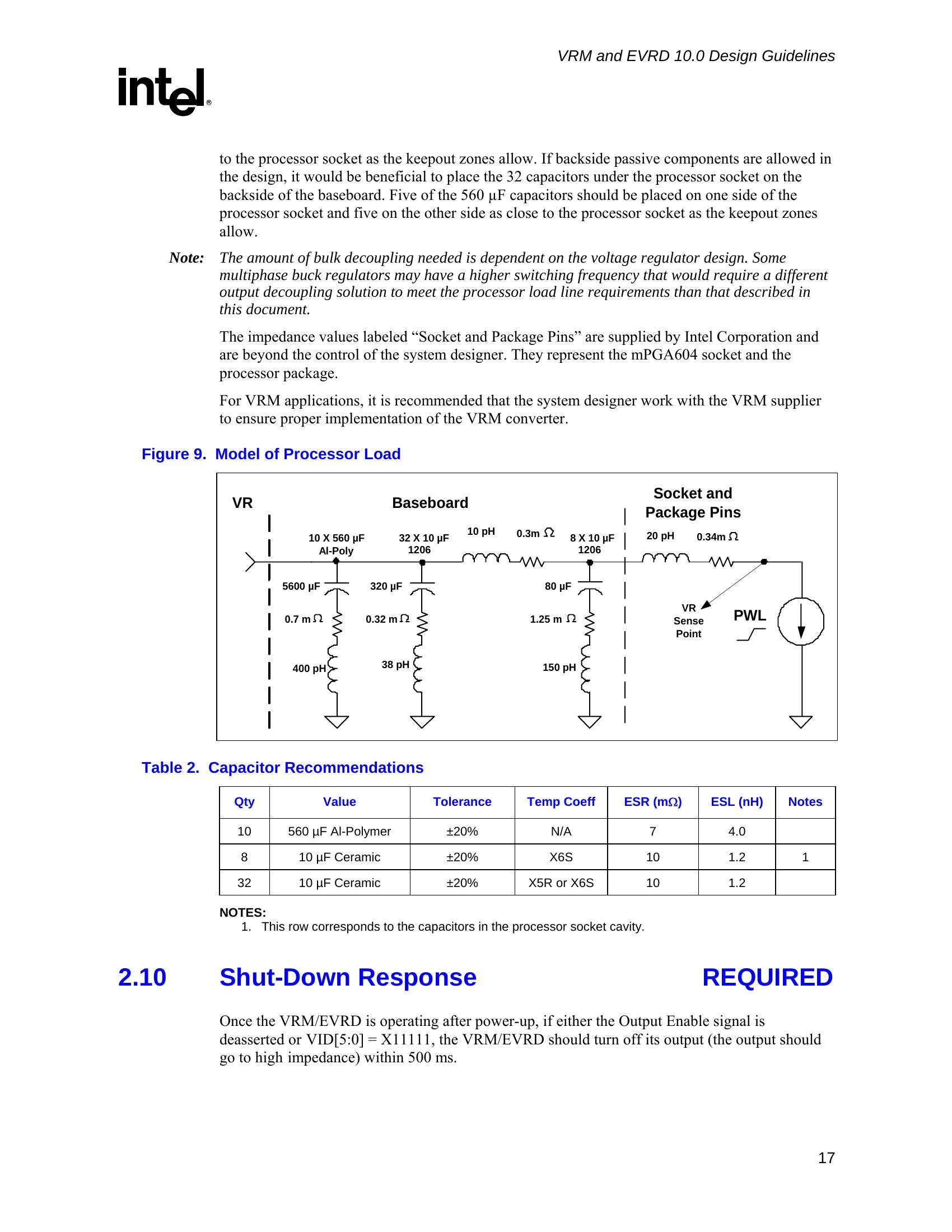
Figure 9 is a representative example of a baseboard decoupling solution and a processor load. The
values shown are for a four–phase switching voltage regulator design . The parasitic baseboard
values are extracted from a design using a four-layer baseboard with 2 ounces total of copper for
Vcc and 2 ounces total of copper for ground. The amount of bulk decoupling required is
dependent on the voltage regulator design.
This design incorporates at least ten 560 µF Aluminum-polymer bulk capacitors and forty 10 µF
ceramic high frequency capacitors per processor (Table 2). Eight of the 10 µF capacitors should
be placed in the cavity of the processor socket. The remaining 32 capacitors should be split
evenly such that half are on one side of the processor socket and half are on the other side as close
16
| None | |
| None | |
| 36 VID steps @ 5 µs each step = 180 µs |
| None | None | None | None | ||
| None | None | None | 0 ns | ||
| None | None | None | None | ase V g tim | |
| wo s | wo s | rst c ettlin | None | None |
| None | |
| None |
VRM and EVRD 10.0 Design Guidelines
R
to the processor socket as the keepout zones allow. If backside passive components are allowed in
the design, it would be beneficial to place the 32 capacitors under the processor socket on the
backside of the baseboard. Five of the 560 µF capacitors should be placed on one side of the
processor socket and five on the other side as close to the processor socket as the keepout zones
allow.
Note: The amount of bulk decoupling needed is dependent on the voltage regulator design. Some
multiphase buck regulators may have a higher switching frequency that would require a different
output decoupling solution to meet the processor load line requirements than that described in
this document.
The impedance values labeled “Socket and Package Pins” are supplied by Intel Corporation and
are beyond the control of the system designer. They represent the mPGA604 socket and the
processor package.
For VRM applications, it is recommended that the system designer work with the VRM supplier
to ensure proper implementation of the VRM converter.
Figure 9. Model of Processor Load
Socket and
VR Baseboard
Package Pins
10 X 560 µF 32 X 10 µF 10 pH 0.3m 8 X 10 µF 20 pH 0.34m
Al-Poly 1206 1206
5600 µF 320 µF 80 µF
VR
PWL
0.7 m 0.32 m 1.25 m Sense
Point
400 pH 38 pH 150 pH
Table 2. Capacitor Recommendations
Qty Value Tolerance Temp Coeff ESR (mΩ) ESL (nH) Notes
10 560 µF Al-Polymer ±20% N/A 7 4.0
8 10 µF Ceramic ±20% X6S 10 1.2 1
32 10 µF Ceramic ±20% X5R or X6S 10 1.2
NOTES:
1. This row corresponds to the capacitors in the processor socket cavity.
2.10 Shut-Down Response REQUIRED
Once the VRM/EVRD is operating after power-up, if either the Output Enable signal is
deasserted or VID[5:0] = X11111, the VRM/EVRD should turn off its output (the output should
go to high impedance) within 500 ms.
17
| None | |
| None | |
| Qty | Value | Tolerance | Temp Coeff | ESR (mΩ) | ESL (nH) | Notes |
| 10 | 560 µF Al-Polymer | ±20% | N/A | 7 | 4.0 | |
| 8 | 10 µF Ceramic | ±20% | X6S | 10 | 1.2 | 1 |
| 32 | 10 µF Ceramic | ±20% | X5R or X6S | 10 | 1.2 |
VRM and EVRD 10.0 Design Guidelines
R
3 Control Signals
3.1 Output Enable (OUTEN) REQUIRED
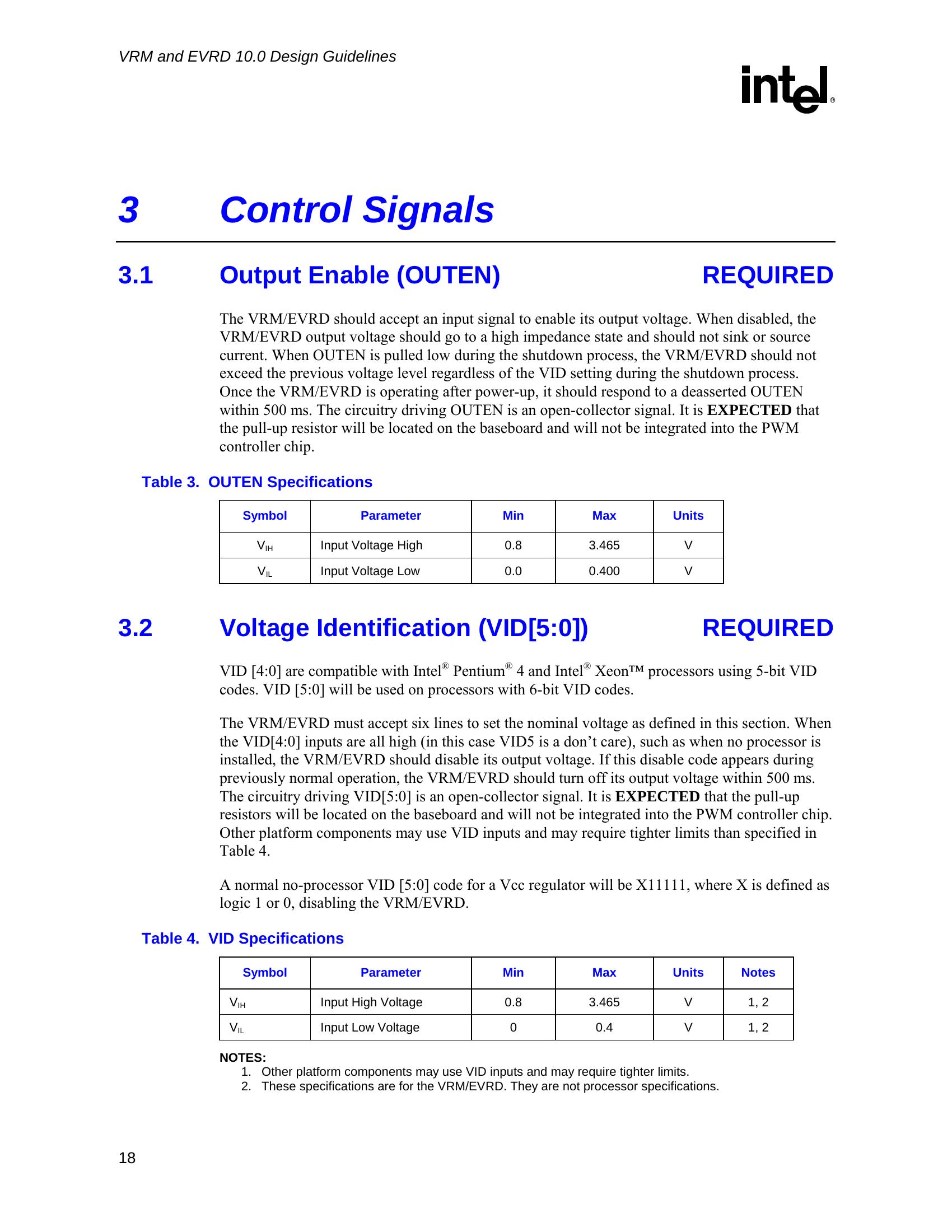
The VRM/EVRD should accept an input signal to enable its output voltage. When disabled, the
VRM/EVRD output voltage should go to a high impedance state and should not sink or source
current. When OUTEN is pulled low during the shutdown process, the VRM/EVRD should not
exceed the previous voltage level regardless of the VID setting during the shutdown process.
Once the VRM/EVRD is operating after power-up, it should respond to a deasserted OUTEN
within 500 ms. The circuitry driving OUTEN is an open-collector signal. It is EXPECTED that
the pull-up resistor will be located on the baseboard and will not be integrated into the PWM
controller chip.
Table 3. OUTEN Specifications
Symbol Parameter Min Max Units
V Input Voltage High 0.8 3.465 V
IH
V Input Voltage Low 0.0 0.400 V
IL
3.2 Voltage Identification (VID[5:0]) REQUIRED
VID [4:0] are compatible with Intel® Pentium® 4 and Intel® Xeon™ processors using 5-bit VID
codes. VID [5:0] will be used on processors with 6-bit VID codes.
The VRM/EVRD must accept six lines to set the nominal voltage as defined in this section. When
the VID[4:0] inputs are all high (in this case VID5 is a don’t care), such as when no processor is
installed, the VRM/EVRD should disable its output voltage. If this disable code appears during
previously normal operation, the VRM/EVRD should turn off its output voltage within 500 ms.
The circuitry driving VID[5:0] is an open-collector signal. It is EXPECTED that the pull-up
resistors will be located on the baseboard and will not be integrated into the PWM controller chip.
Other platform components may use VID inputs and may require tighter limits than specified in
Table 4.
A normal no-processor VID [5:0] code for a Vcc regulator will be X11111, where X is defined as
logic 1 or 0, disabling the VRM/EVRD.
Table 4. VID Specifications
Symbol Parameter Min Max Units Notes
V Input High Voltage 0.8 3.465 V 1, 2
IH
V Input Low Voltage 0 0.4 V 1, 2
IL
NOTES:
1. Other platform components may use VID inputs and may require tighter limits.
2. These specifications are for the VRM/EVRD. They are not processor specifications.
18
| None | |
| Symbol | Parameter | Min | Max | Units |
| V IH | Input Voltage High | 0.8 | 3.465 | V |
| V IL | Input Voltage Low | 0.0 | 0.400 | V |
| Symbol | Parameter | Min | Max | Units | Notes |
| V IH | Input High Voltage | 0.8 | 3.465 | V | 1, 2 |
| V IL | Input Low Voltage | 0 | 0.4 | V | 1, 2 |
VRM and EVRD 10.0 Design Guidelines
R
Table 5. Voltage Identification (VID)
Processor Pins (0 = low, 1 = high) Vout Processor Pins (0 = low, 1 = high) Vout
(V) (V)
VID4 VID3 VID2 VID1 VID0 VID5 VID4 VID3 VID2 VID1 VID0 VID5
0 1 0 1 0 0 0.8375 1 1 0 1 0 0 1.2125
0 1 0 0 1 1 0.8500 1 1 0 0 1 1 1.2250
0 1 0 0 1 0 0.8625 1 1 0 0 1 0 1.2375
0 1 0 0 0 1 0.8750 1 1 0 0 0 1 1.2500
0 1 0 0 0 0 0.8875 1 1 0 0 0 0 1.2625
0 0 1 1 1 1 0.9000 1 0 1 1 1 1 1.2750
0 0 1 1 1 0 0.9125 1 0 1 1 1 0 1.2875
0 0 1 1 0 1 0.9250 1 0 1 1 0 1 1.3000
0 0 1 1 0 0 0.9375 1 0 1 1 0 0 1.3125
0 0 1 0 1 1 0.9500 1 0 1 0 1 1 1.3250
0 0 1 0 1 0 0.9625 1 0 1 0 1 0 1.3375
0 0 1 0 0 1 0.9750 1 0 1 0 0 1 1.3500
0 0 1 0 0 0 0.9875 1 0 1 0 0 0 1.3625
0 0 0 1 1 1 1.0000 1 0 0 1 1 1 1.3750
0 0 0 1 1 0 1.0125 1 0 0 1 1 0 1.3875
0 0 0 1 0 1 1.0250 1 0 0 1 0 1 1.4000
0 0 0 1 0 0 1.0375 1 0 0 1 0 0 1.4125
0 0 0 0 1 1 1.0500 1 0 0 0 1 1 1.4250
0 0 0 0 1 0 1.0625 1 0 0 0 1 0 1.4375
0 0 0 0 0 1 1.0750 1 0 0 0 0 1 1.4500
0 0 0 0 0 0 1.0875 1 0 0 0 0 0 1.4625
1 1 1 1 1 1 OFF1 0 1 1 1 1 1 1.4750
1 1 1 1 1 0 OFF1 0 1 1 1 1 0 1.4875
1 1 1 1 0 1 1.1000 0 1 1 1 0 1 1.5000
1 1 1 1 0 0 1.1125 0 1 1 1 0 0 1.5125
1 1 1 0 1 1 1.1250 0 1 1 0 1 1 1.5250
1 1 1 0 1 0 1.1375 0 1 1 0 1 0 1.5375
1 1 1 0 0 1 1.1500 0 1 1 0 0 1 1.5500
1 1 1 0 0 0 1.1625 0 1 1 0 0 0 1.5625
1 1 0 1 1 1 1.1750 0 1 0 1 1 1 1.5750
1 1 0 1 1 0 1.1875 0 1 0 1 1 0 1.5875
1 1 0 1 0 1 1.2000 0 1 0 1 0 1 1.6000
NOTE:
3. Output disabled – the same as deasserting the Output Enable input (Section 3.1).
19
| None | |
| None | |
| Processor Pins (0 = low, 1 = high) | None | None | None | None | None | Vout (V) | Processor Pins (0 = low, 1 = high) | None | None | None | None | None | Vout (V) |
| VID4 | VID3 | VID2 | VID1 | VID0 | VID5 | None | VID4 | VID3 | VID2 | VID1 | VID0 | VID5 | None |
| 0 | 1 | 0 | 1 | 0 | 0 | 0.8375 | 1 | 1 | 0 | 1 | 0 | 0 | 1.2125 |
| 0 | 1 | 0 | 0 | 1 | 1 | 0.8500 | 1 | 1 | 0 | 0 | 1 | 1 | 1.2250 |
| 0 | 1 | 0 | 0 | 1 | 0 | 0.8625 | 1 | 1 | 0 | 0 | 1 | 0 | 1.2375 |
| 0 | 1 | 0 | 0 | 0 | 1 | 0.8750 | 1 | 1 | 0 | 0 | 0 | 1 | 1.2500 |
| 0 | 1 | 0 | 0 | 0 | 0 | 0.8875 | 1 | 1 | 0 | 0 | 0 | 0 | 1.2625 |
| 0 | 0 | 1 | 1 | 1 | 1 | 0.9000 | 1 | 0 | 1 | 1 | 1 | 1 | 1.2750 |
| 0 | 0 | 1 | 1 | 1 | 0 | 0.9125 | 1 | 0 | 1 | 1 | 1 | 0 | 1.2875 |
| 0 | 0 | 1 | 1 | 0 | 1 | 0.9250 | 1 | 0 | 1 | 1 | 0 | 1 | 1.3000 |
| 0 | 0 | 1 | 1 | 0 | 0 | 0.9375 | 1 | 0 | 1 | 1 | 0 | 0 | 1.3125 |
| 0 | 0 | 1 | 0 | 1 | 1 | 0.9500 | 1 | 0 | 1 | 0 | 1 | 1 | 1.3250 |
| 0 | 0 | 1 | 0 | 1 | 0 | 0.9625 | 1 | 0 | 1 | 0 | 1 | 0 | 1.3375 |
| 0 | 0 | 1 | 0 | 0 | 1 | 0.9750 | 1 | 0 | 1 | 0 | 0 | 1 | 1.3500 |
| 0 | 0 | 1 | 0 | 0 | 0 | 0.9875 | 1 | 0 | 1 | 0 | 0 | 0 | 1.3625 |
| 0 | 0 | 0 | 1 | 1 | 1 | 1.0000 | 1 | 0 | 0 | 1 | 1 | 1 | 1.3750 |
| 0 | 0 | 0 | 1 | 1 | 0 | 1.0125 | 1 | 0 | 0 | 1 | 1 | 0 | 1.3875 |
| 0 | 0 | 0 | 1 | 0 | 1 | 1.0250 | 1 | 0 | 0 | 1 | 0 | 1 | 1.4000 |
| 0 | 0 | 0 | 1 | 0 | 0 | 1.0375 | 1 | 0 | 0 | 1 | 0 | 0 | 1.4125 |
| 0 | 0 | 0 | 0 | 1 | 1 | 1.0500 | 1 | 0 | 0 | 0 | 1 | 1 | 1.4250 |
| 0 | 0 | 0 | 0 | 1 | 0 | 1.0625 | 1 | 0 | 0 | 0 | 1 | 0 | 1.4375 |
| 0 | 0 | 0 | 0 | 0 | 1 | 1.0750 | 1 | 0 | 0 | 0 | 0 | 1 | 1.4500 |
| 0 | 0 | 0 | 0 | 0 | 0 | 1.0875 | 1 | 0 | 0 | 0 | 0 | 0 | 1.4625 |
| 1 | 1 | 1 | 1 | 1 | 1 | OFF1 | 0 | 1 | 1 | 1 | 1 | 1 | 1.4750 |
| 1 | 1 | 1 | 1 | 1 | 0 | OFF1 | 0 | 1 | 1 | 1 | 1 | 0 | 1.4875 |
| 1 | 1 | 1 | 1 | 0 | 1 | 1.1000 | 0 | 1 | 1 | 1 | 0 | 1 | 1.5000 |
| 1 | 1 | 1 | 1 | 0 | 0 | 1.1125 | 0 | 1 | 1 | 1 | 0 | 0 | 1.5125 |
| 1 | 1 | 1 | 0 | 1 | 1 | 1.1250 | 0 | 1 | 1 | 0 | 1 | 1 | 1.5250 |
| 1 | 1 | 1 | 0 | 1 | 0 | 1.1375 | 0 | 1 | 1 | 0 | 1 | 0 | 1.5375 |
| 1 | 1 | 1 | 0 | 0 | 1 | 1.1500 | 0 | 1 | 1 | 0 | 0 | 1 | 1.5500 |
| 1 | 1 | 1 | 0 | 0 | 0 | 1.1625 | 0 | 1 | 1 | 0 | 0 | 0 | 1.5625 |
| 1 | 1 | 0 | 1 | 1 | 1 | 1.1750 | 0 | 1 | 0 | 1 | 1 | 1 | 1.5750 |
| 1 | 1 | 0 | 1 | 1 | 0 | 1.1875 | 0 | 1 | 0 | 1 | 1 | 0 | 1.5875 |
| 1 | 1 | 0 | 1 | 0 | 1 | 1.2000 | 0 | 1 | 0 | 1 | 0 | 1 | 1.6000 |
VRM and EVRD 10.0 Design Guidelines
R
3.3 Differential Remote Sense (VO_SEN+/–) REQUIRED
The PWM controller will include differential sense inputs to compensate for an output voltage
offset of <300 mV in the power distribution path. This common mode voltage is expected to
occur due to transient currents and parasitic inductances and is not expected to be caused by
parasitic resistances. The remote sense lines should draw no more than 10 mA, to minimize offset
errors.
3.4 VRM Present (VRM_pres#) EXPECTED
The VRM should have the VRM_pres# signal. This signal is an output signal used to indicate to
the system that a VRM is plugged into the socket. VRM_pres# is an open-collector/drain or
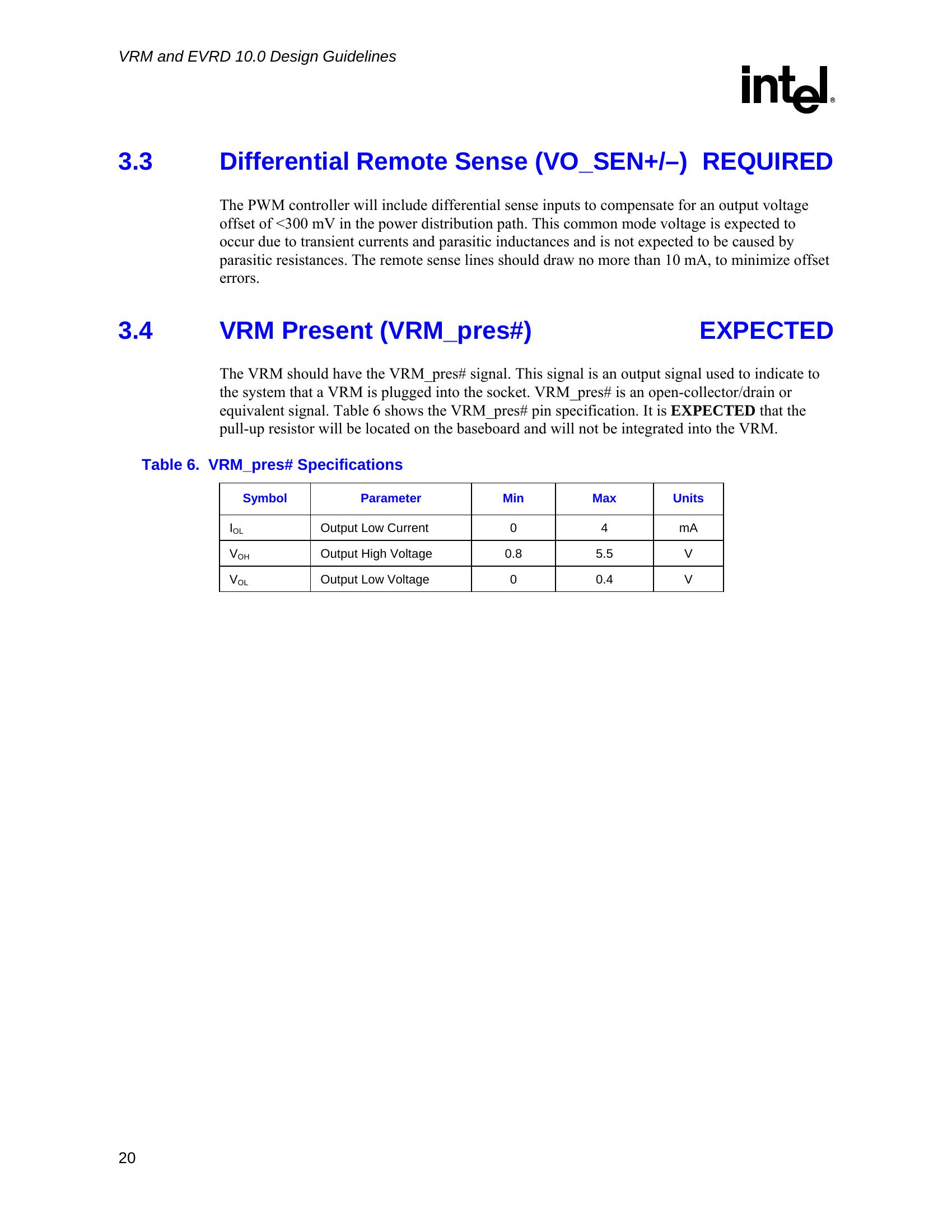
equivalent signal. Table 6 shows the VRM_pres# pin specification. It is EXPECTED that the
pull-up resistor will be located on the baseboard and will not be integrated into the VRM.
Table 6. VRM_pres# Specifications
Symbol Parameter Min Max Units
I Output Low Current 0 4 mA
OL
V Output High Voltage 0.8 5.5 V
OH
V Output Low Voltage 0 0.4 V
OL
20
| None | |
| None | |
| Symbol | Parameter | Min | Max | Units |
| I OL | Output Low Current | 0 | 4 | mA |
| V OH | Output High Voltage | 0.8 | 5.5 | V |
| V OL | Output Low Voltage | 0 | 0.4 | V |
VRM and EVRD 10.0 Design Guidelines
R
21
| None | |
| None | |

VRM and EVRD 10.0 Design Guidelines
R
4 Input Voltage and Current
4.1 Input Voltages EXPECTED
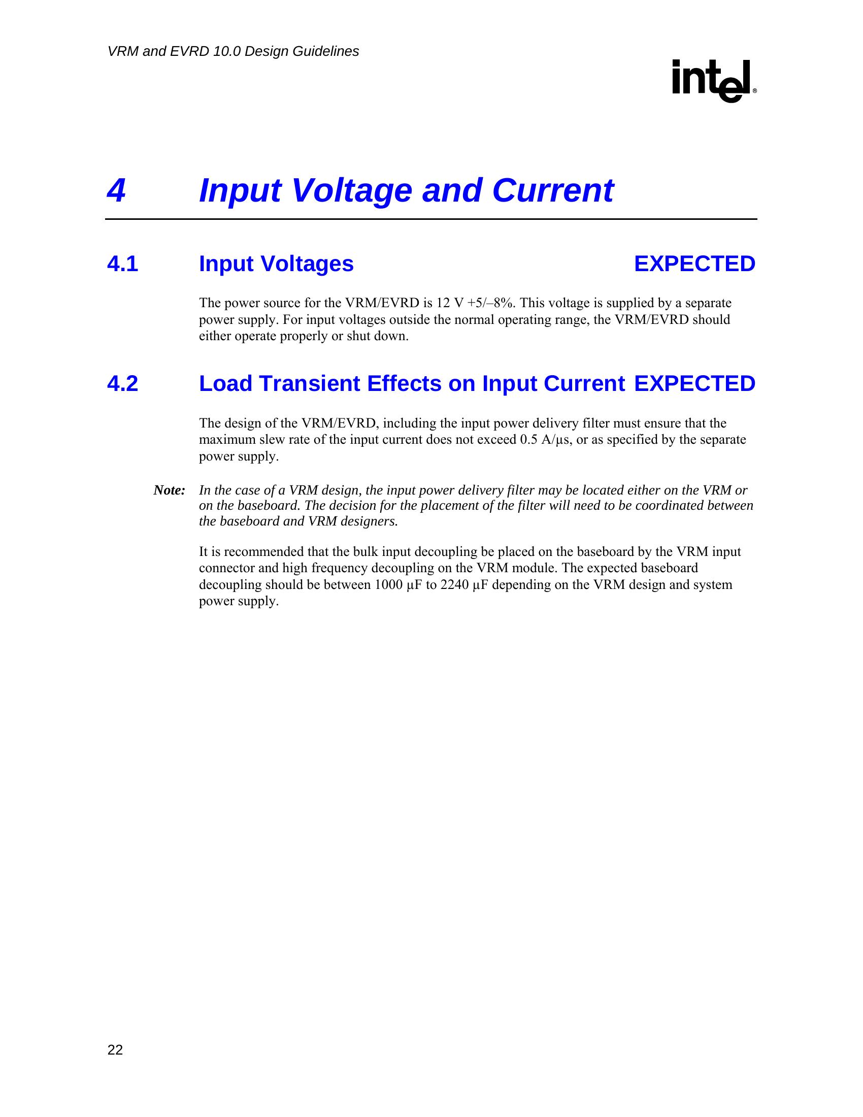
The power source for the VRM/EVRD is 12 V +5/–8%. This voltage is supplied by a separate
power supply. For input voltages outside the normal operating range, the VRM/EVRD should
either operate properly or shut down.
4.2 Load Transient Effects on Input Current EXPECTED
The design of the VRM/EVRD, including the input power delivery filter must ensure that the
maximum slew rate of the input current does not exceed 0.5 A/µs, or as specified by the separate
power supply.
Note: In the case of a VRM design, the input power delivery filter may be located either on the VRM or
on the baseboard. The decision for the placement of the filter will need to be coordinated between
the baseboard and VRM designers.
It is recommended that the bulk input decoupling be placed on the baseboard by the VRM input
connector and high frequency decoupling on the VRM module. The expected baseboard
decoupling should be between 1000 µF to 2240 µF depending on the VRM design and system
power supply.
22
| None | |
| None | |
VRM and EVRD 10.0 Design Guidelines
R
23
| None | |
| None | |

VRM and EVRD 10.0 Design Guidelines
R
5 Processor Voltage Output
Protection
These are features built into the VRM/EVRD to help prevent damage to itself, the processor, or
other system components.
5.1 Over-Voltage Protection (OVP) PROPOSED
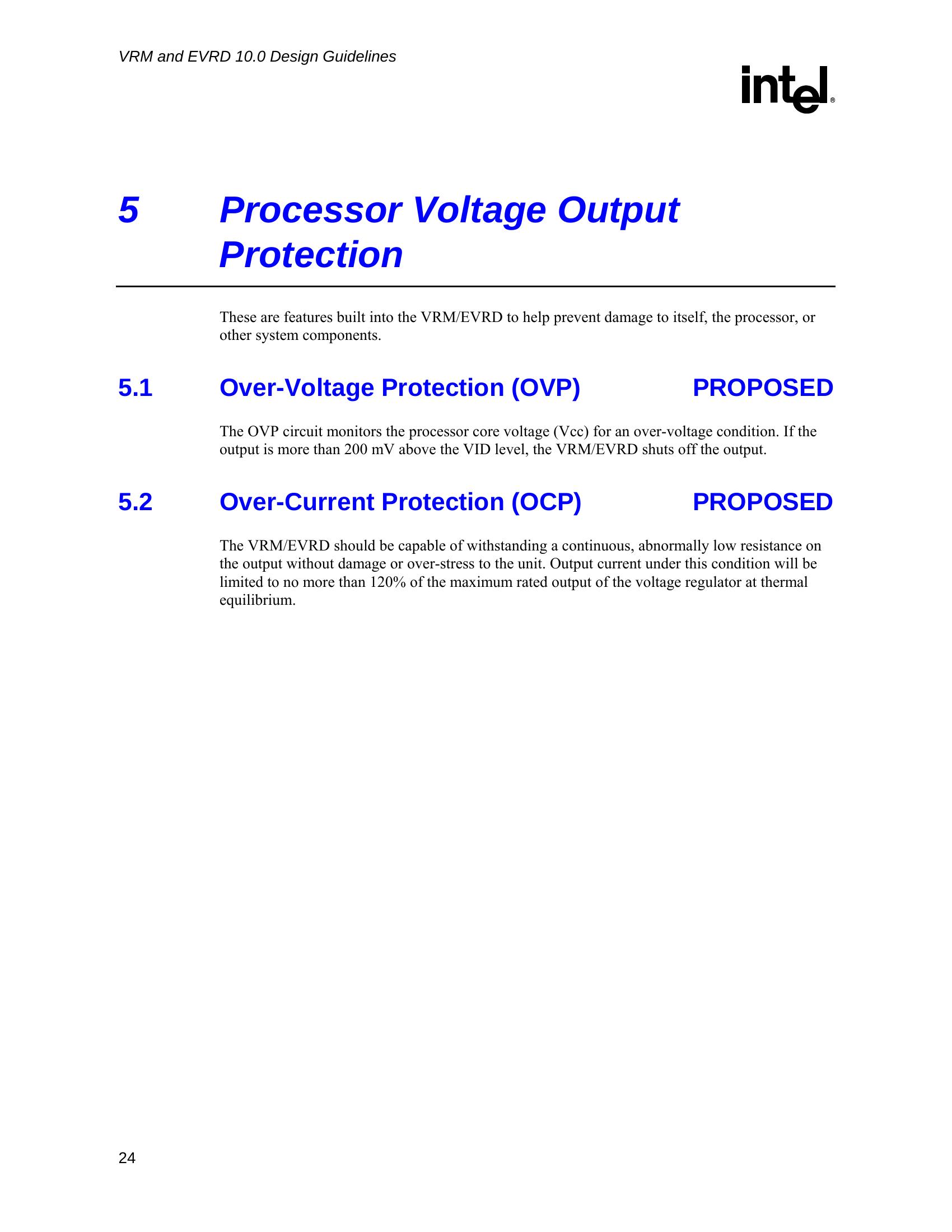
The OVP circuit monitors the processor core voltage (Vcc) for an over-voltage condition. If the
output is more than 200 mV above the VID level, the VRM/EVRD shuts off the output.
5.2 Over-Current Protection (OCP) PROPOSED
The VRM/EVRD should be capable of withstanding a continuous, abnormally low resistance on
the output without damage or over-stress to the unit. Output current under this condition will be
limited to no more than 120% of the maximum rated output of the voltage regulator at thermal
equilibrium.
24
| None | |
| None | |
VRM and EVRD 10.0 Design Guidelines
R
25
| None | |
| None | |

VRM and EVRD 10.0 Design Guidelines
R
6 Output Indicators
6.1 Vcc Power-Good (Vcc_PWRGD) PROPOSED
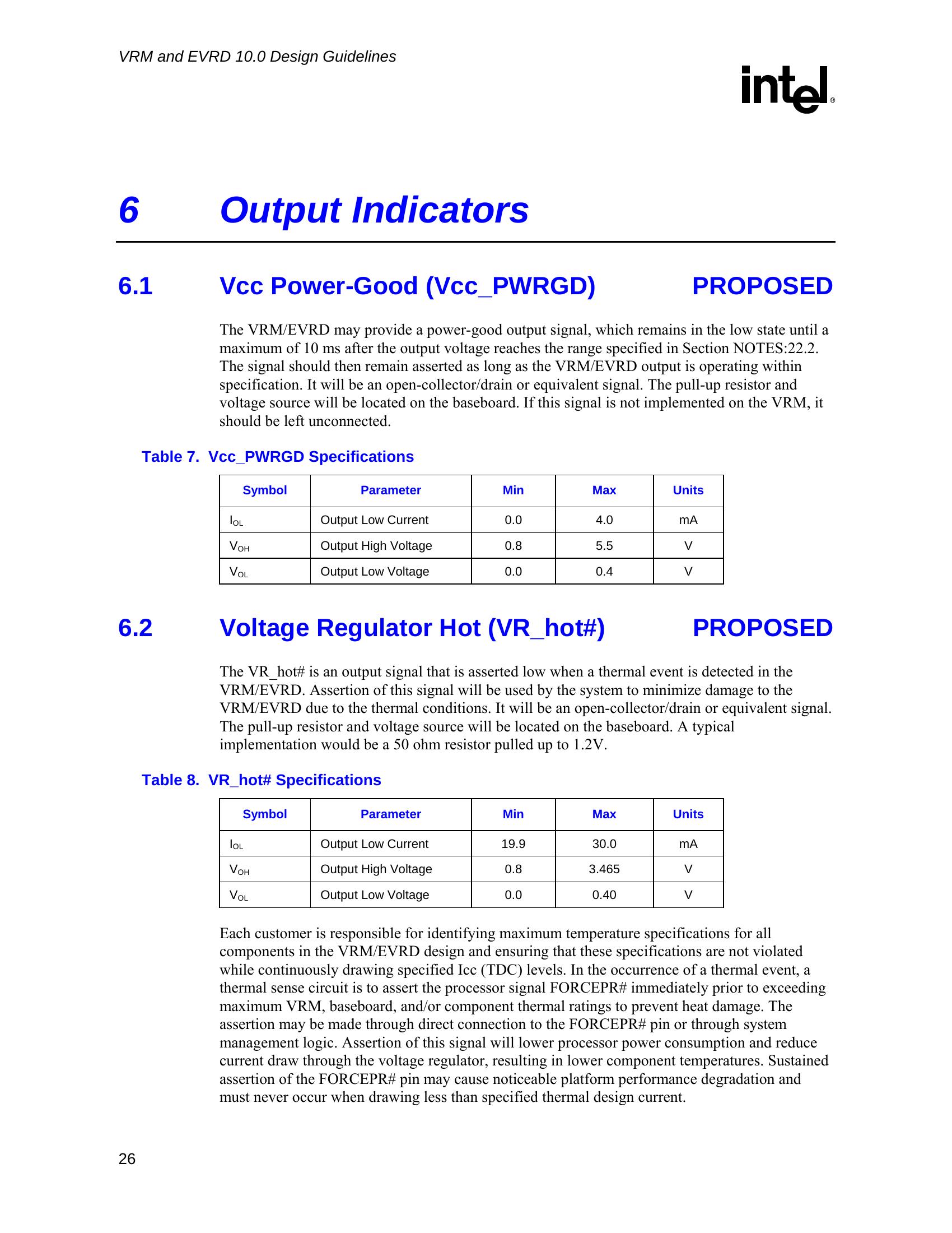
The VRM/EVRD may provide a power-good output signal, which remains in the low state until a
maximum of 10 ms after the output voltage reaches the range specified in Section NOTES:22.2.
The signal should then remain asserted as long as the VRM/EVRD output is operating within
specification. It will be an open-collector/drain or equivalent signal. The pull-up resistor and
voltage source will be located on the baseboard. If this signal is not implemented on the VRM, it
should be left unconnected.
Table 7. Vcc_PWRGD Specifications
Symbol Parameter Min Max Units
I Output Low Current 0.0 4.0 mA
OL
V Output High Voltage 0.8 5.5 V
OH
V Output Low Voltage 0.0 0.4 V
OL
6.2 Voltage Regulator Hot (VR_hot#) PROPOSED
The VR_hot# is an output signal that is asserted low when a thermal event is detected in the
VRM/EVRD. Assertion of this signal will be used by the system to minimize damage to the
VRM/EVRD due to the thermal conditions. It will be an open-collector/drain or equivalent signal.
The pull-up resistor and voltage source will be located on the baseboard. A typical
implementation would be a 50 ohm resistor pulled up to 1.2V.
Table 8. VR_hot# Specifications
Symbol Parameter Min Max Units
I Output Low Current 19.9 30.0 mA
OL
V Output High Voltage 0.8 3.465 V
OH
V Output Low Voltage 0.0 0.40 V
OL
Each customer is responsible for identifying maximum temperature specifications for all
components in the VRM/EVRD design and ensuring that these specifications are not violated
while continuously drawing specified Icc (TDC) levels. In the occurrence of a thermal event, a
thermal sense circuit is to assert the processor signal FORCEPR# immediately prior to exceeding
maximum VRM, baseboard, and/or component thermal ratings to prevent heat damage. The
assertion may be made through direct connection to the FORCEPR# pin or through system
management logic. Assertion of this signal will lower processor power consumption and reduce
current draw through the voltage regulator, resulting in lower component temperatures. Sustained
assertion of the FORCEPR# pin may cause noticeable platform performance degradation and
must never occur when drawing less than specified thermal design current.
26
| None | |
| None | |
| Symbol | Parameter | Min | Max | Units |
| I OL | Output Low Current | 0.0 | 4.0 | mA |
| V OH | Output High Voltage | 0.8 | 5.5 | V |
| V OL | Output Low Voltage | 0.0 | 0.4 | V |
| Symbol | Parameter | Min | Max | Units |
| I OL | Output Low Current | 19.9 | 30.0 | mA |
| V OH | Output High Voltage | 0.8 | 3.465 | V |
| V OL | Output Low Voltage | 0.0 | 0.40 | V |
VRM and EVRD 10.0 Design Guidelines
R
It is recommended that hysteresis be designed into the thermal sense circuit to prevent a scenario
in which the VR_hot# signal is rapidly being asserted and deasserted.
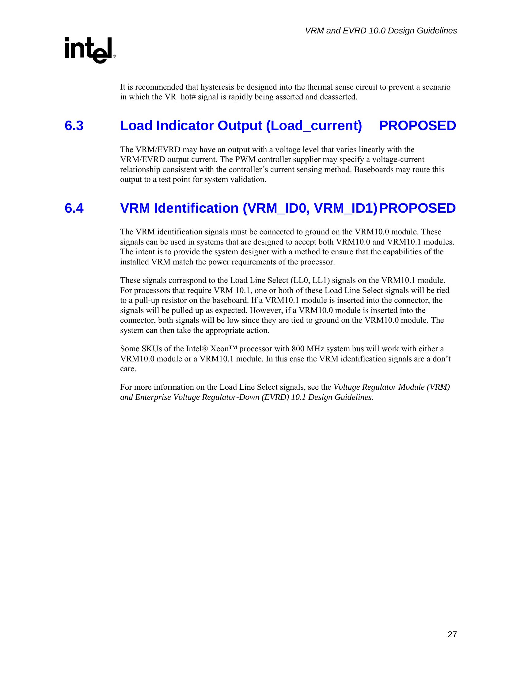
6.3 Load Indicator Output (Load_current) PROPOSED
The VRM/EVRD may have an output with a voltage level that varies linearly with the
VRM/EVRD output current. The PWM controller supplier may specify a voltage-current
relationship consistent with the controller’s current sensing method. Baseboards may route this
output to a test point for system validation.
6.4 VRM Identification (VRM_ID0, VRM_ID1) PROPOSED
The VRM identification signals must be connected to ground on the VRM10.0 module. These
signals can be used in systems that are designed to accept both VRM10.0 and VRM10.1 modules.
The intent is to provide the system designer with a method to ensure that the capabilities of the
installed VRM match the power requirements of the processor.
These signals correspond to the Load Line Select (LL0, LL1) signals on the VRM10.1 module.
For processors that require VRM 10.1, one or both of these Load Line Select signals will be tied
to a pull-up resistor on the baseboard. If a VRM10.1 module is inserted into the connector, the
signals will be pulled up as expected. However, if a VRM10.0 module is inserted into the
connector, both signals will be low since they are tied to ground on the VRM10.0 module. The
system can then take the appropriate action.
Some SKUs of the Intel® Xeon™ processor with 800 MHz system bus will work with either a
VRM10.0 module or a VRM10.1 module. In this case the VRM identification signals are a don’t
care.
For more information on the Load Line Select signals, see the Voltage Regulator Module (VRM)
and Enterprise Voltage Regulator-Down (EVRD) 10.1 Design Guidelines.
27
| None | |
| None | |
VRM and EVRD 10.0 Design Guidelines
R
7 VRM – Mechanical Guidelines
7.1 VRM Connector EXPECTED
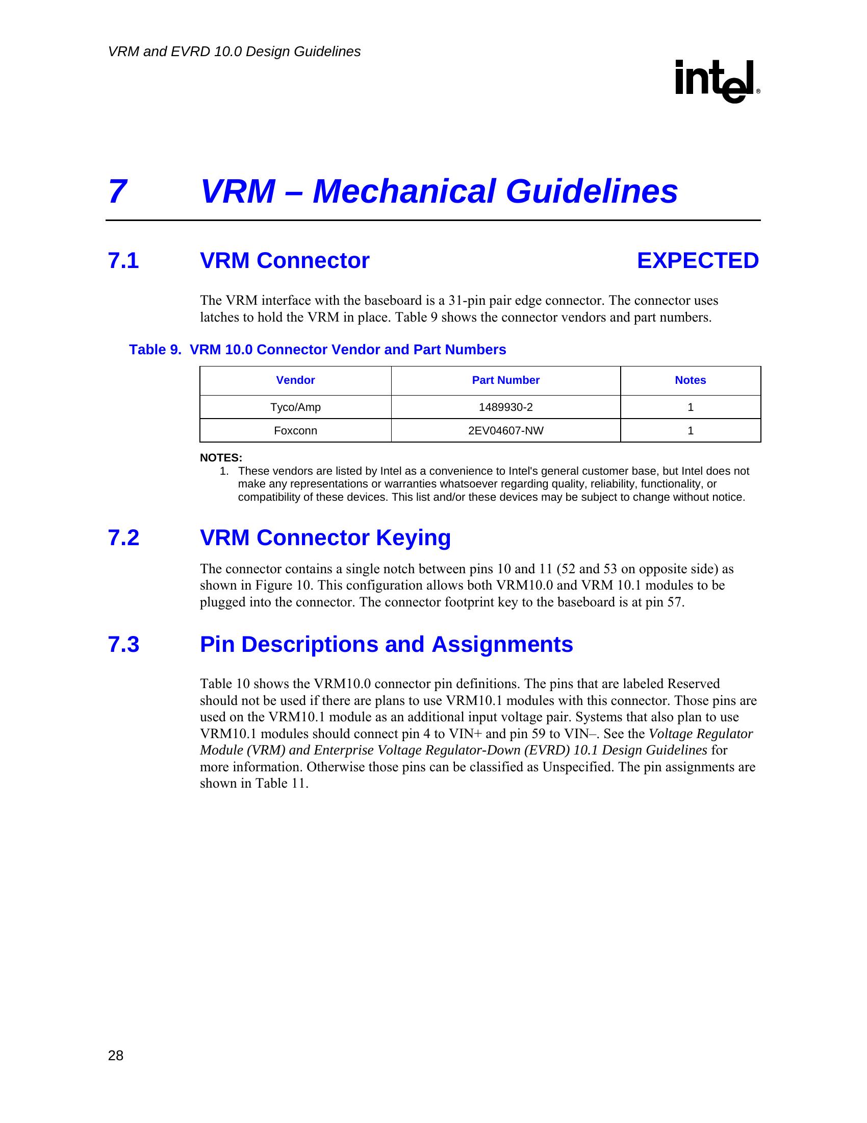
The VRM interface with the baseboard is a 31-pin pair edge connector. The connector uses
latches to hold the VRM in place. Table 9 shows the connector vendors and part numbers.
Table 9. VRM 10.0 Connector Vendor and Part Numbers
Vendor Part Number Notes
Tyco/Amp 1489930-2 1
Foxconn 2EV04607-NW 1
NOTES:
1. These vendors are listed by Intel as a convenience to Intel’s general customer base, but Intel does not
make any representations or warranties whatsoever regarding quality, reliability, functionality, or
compatibility of these devices. This list and/or these devices may be subject to change without notice.
7.2 VRM Connector Keying
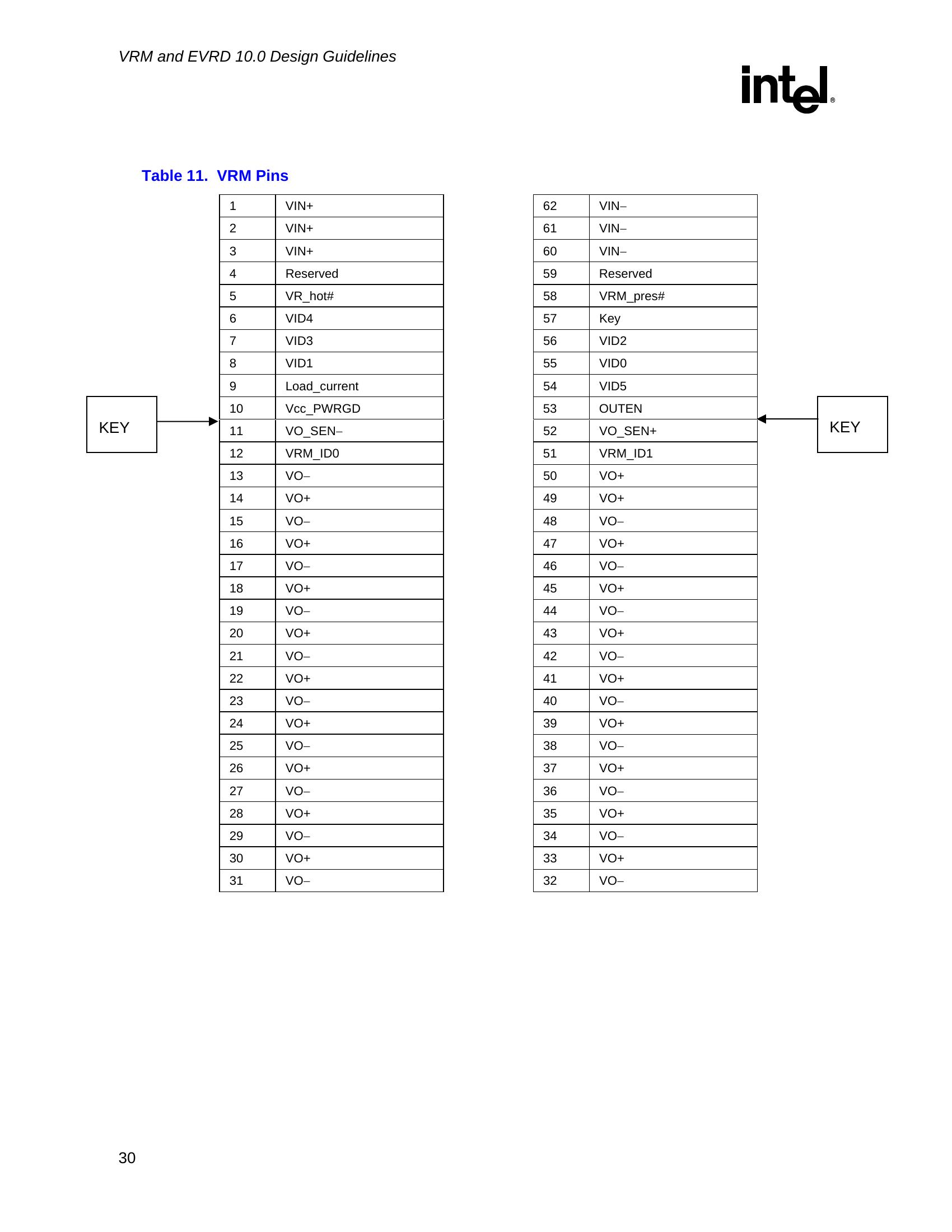
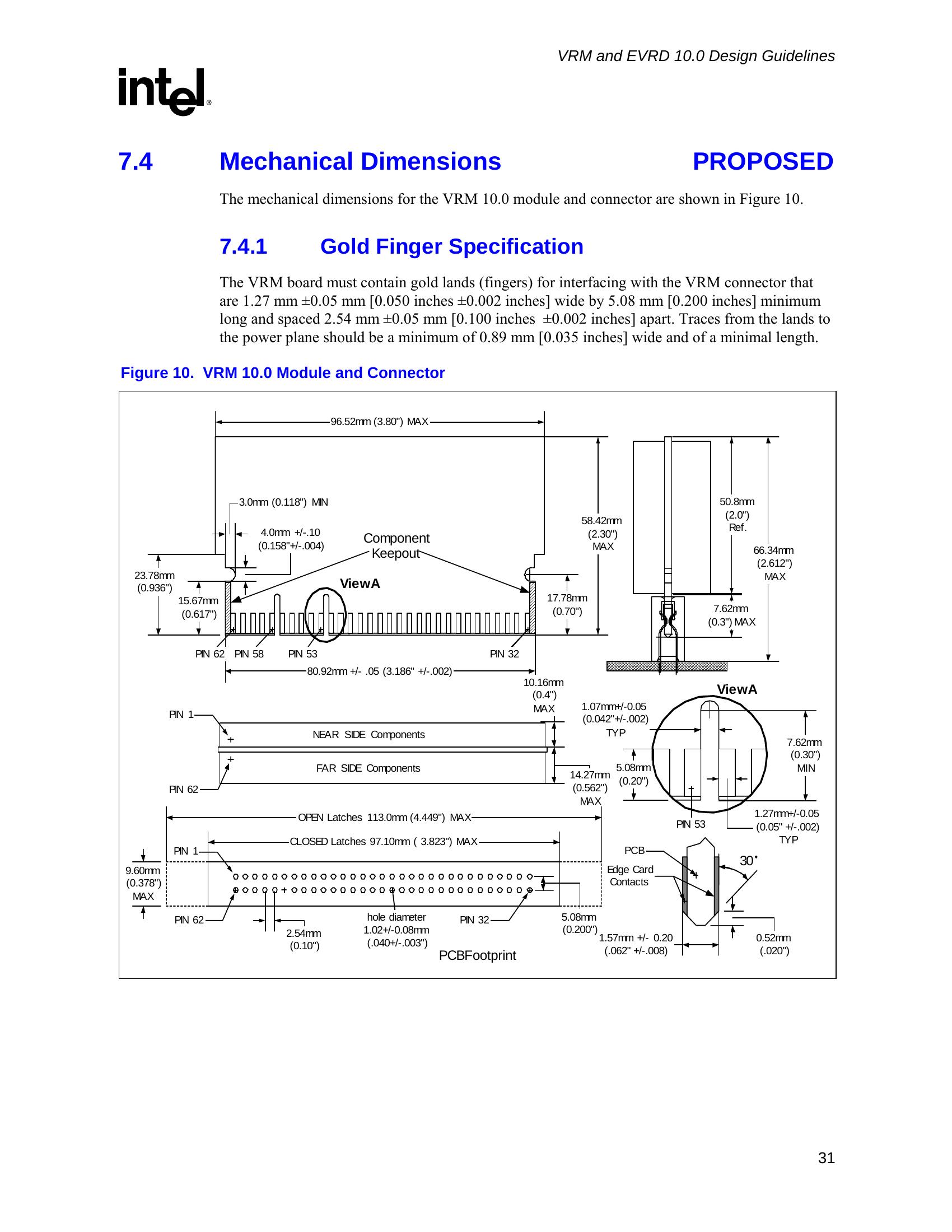
The connector contains a single notch between pins 10 and 11 (52 and 53 on opposite side) as
shown in Figure 10. This configuration allows both VRM10.0 and VRM 10.1 modules to be
plugged into the connector. The connector footprint key to the baseboard is at pin 57.
7.3 Pin Descriptions and Assignments
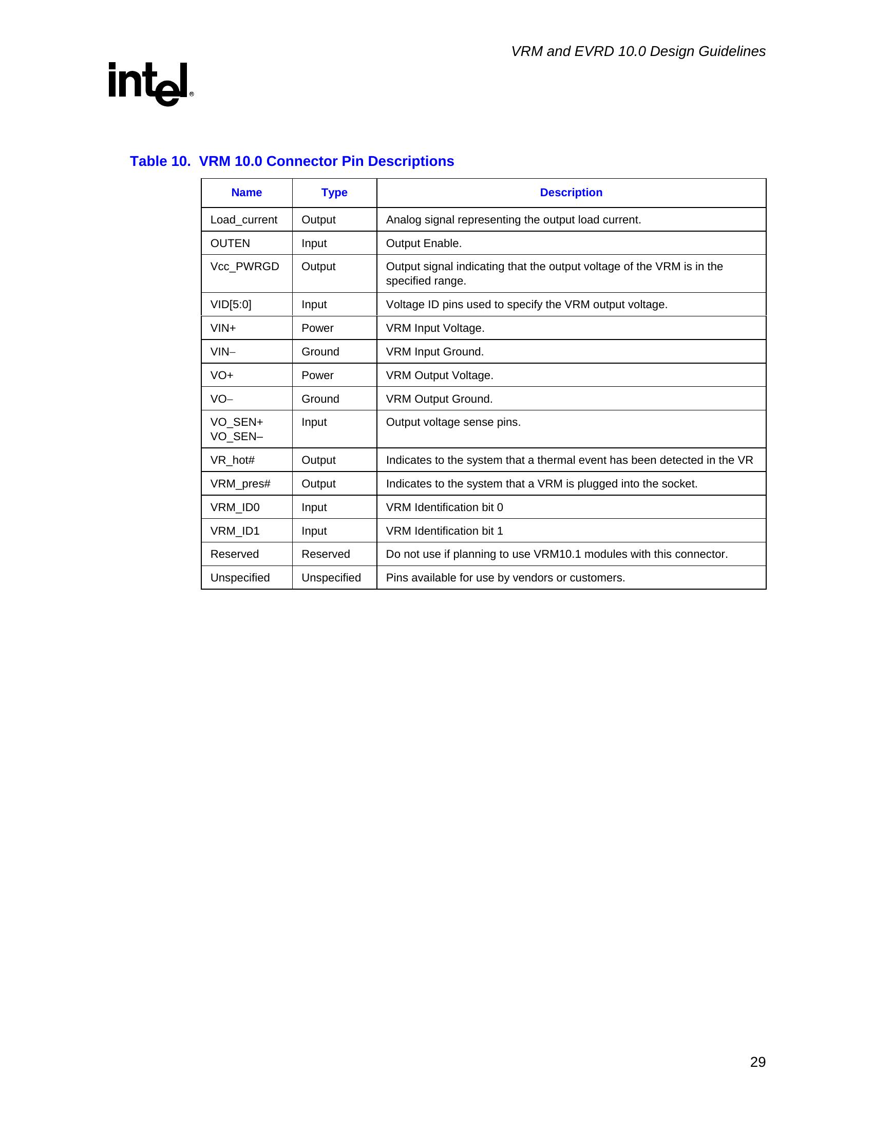
Table 10 shows the VRM10.0 connector pin definitions. The pins that are labeled Reserved
should not be used if there are plans to use VRM10.1 modules with this connector. Those pins are
used on the VRM10.1 module as an additional input voltage pair. Systems that also plan to use
VRM10.1 modules should connect pin 4 to VIN+ and pin 59 to VIN–. See the Voltage Regulator
Module (VRM) and Enterprise Voltage Regulator-Down (EVRD) 10.1 Design Guidelines for
more information. Otherwise those pins can be classified as Unspecified. The pin assignments are
shown in Table 11.
28
| None | |
| None | |
| Vendor | Part Number | Notes |
| Tyco/Amp | 1489930-2 | 1 |
| Foxconn | 2EV04607-NW | 1 |
VRM and EVRD 10.0 Design Guidelines
R
Table 10. VRM 10.0 Connector Pin Descriptions
Name Type Description
Load_current Output Analog signal representing the output load current.
OUTEN Input Output Enable.
Vcc_PWRGD Output Output signal indicating that the output voltage of the VRM is in the
specified range.
VID[5:0] Input Voltage ID pins used to specify the VRM output voltage.
VIN+ Power VRM Input Voltage.
VIN− Ground VRM Input Ground.
VO+ Power VRM Output Voltage.
VO− Ground VRM Output Ground.
VO_SEN+ Input Output voltage sense pins.
VO_SEN–
VR_hot# Output Indicates to the system that a thermal event has been detected in the VR
VRM_pres# Output Indicates to the system that a VRM is plugged into the socket.
VRM_ID0 Input VRM Identification bit 0
VRM_ID1 Input VRM Identification bit 1
Reserved Reserved Do not use if planning to use VRM10.1 modules with this connector.
Unspecified Unspecified Pins available for use by vendors or customers.
29
| None | |
| None | |
| Name | Type | Description |
| Load_current | Output | Analog signal representing the output load current. |
| OUTEN | Input | Output Enable. |
| Vcc_PWRGD | Output | Output signal indicating that the output voltage of the VRM is in the specified range. |
| VID[5:0] | Input | Voltage ID pins used to specify the VRM output voltage. |
| VIN+ | Power | VRM Input Voltage. |
| VIN− | Ground | VRM Input Ground. |
| VO+ | Power | VRM Output Voltage. |
| VO− | Ground | VRM Output Ground. |
| VO_SEN+ VO_SEN– | Input | Output voltage sense pins. |
| VR_hot# | Output | Indicates to the system that a thermal event has been detected in the VR |
| VRM_pres# | Output | Indicates to the system that a VRM is plugged into the socket. |
| VRM_ID0 | Input | VRM Identification bit 0 |
| VRM_ID1 | Input | VRM Identification bit 1 |
| Reserved | Reserved | Do not use if planning to use VRM10.1 modules with this connector. |
| Unspecified | Unspecified | Pins available for use by vendors or customers. |
VRM and EVRD 10.0 Design Guidelines
R
Table 11. VRM Pins
1 VIN+ 62 VIN−
2 VIN+ 61 VIN−
3 VIN+ 60 VIN−
4 Reserved 59 Reserved
5 VR_hot# 58 VRM_pres#
6 VID4 57 Key
7 VID3 56 VID2
8 VID1 55 VID0
9 Load_current 54 VID5
10 Vcc_PWRGD 53 OUTEN
KEY KEY
11 VO_SEN− 52 VO_SEN+
12 VRM_ID0 51 VRM_ID1
13 VO− 50 VO+
14 VO+ 49 VO+
15 VO− 48 VO−
16 VO+ 47 VO+
17 VO− 46 VO−
18 VO+ 45 VO+
19 VO− 44 VO−
20 VO+ 43 VO+
21 VO− 42 VO−
22 VO+ 41 VO+
23 VO− 40 VO−
24 VO+ 39 VO+
25 VO− 38 VO−
26 VO+ 37 VO+
27 VO− 36 VO−
28 VO+ 35 VO+
29 VO− 34 VO−
30 VO+ 33 VO+
31 VO− 32 VO−
30
| None | |
| 1 | VIN+ |
| 2 | VIN+ |
| 3 | VIN+ |
| 4 | Reserved |
| 5 | VR_hot# |
| 6 | VID4 |
| 7 | VID3 |
| 8 | VID1 |
| 9 | Load_current |
| 10 | Vcc_PWRGD |
| 11 | VO_SEN− |
| 12 | VRM_ID0 |
| 13 | VO− |
| 14 | VO+ |
| 15 | VO− |
| 16 | VO+ |
| 17 | VO− |
| 18 | VO+ |
| 19 | VO− |
| 20 | VO+ |
| 21 | VO− |
| 22 | VO+ |
| 23 | VO− |
| 24 | VO+ |
| 25 | VO− |
| 26 | VO+ |
| 27 | VO− |
| 28 | VO+ |
| 29 | VO− |
| 30 | VO+ |
| 31 | VO− |
| 62 | VIN− |
| 61 | VIN− |
| 60 | VIN− |
| 59 | Reserved |
| 58 | VRM_pres# |
| 57 | Key |
| 56 | VID2 |
| 55 | VID0 |
| 54 | VID5 |
| 53 | OUTEN |
| 52 | VO_SEN+ |
| 51 | VRM_ID1 |
| 50 | VO+ |
| 49 | VO+ |
| 48 | VO− |
| 47 | VO+ |
| 46 | VO− |
| 45 | VO+ |
| 44 | VO− |
| 43 | VO+ |
| 42 | VO− |
| 41 | VO+ |
| 40 | VO− |
| 39 | VO+ |
| 38 | VO− |
| 37 | VO+ |
| 36 | VO− |
| 35 | VO+ |
| 34 | VO− |
| 33 | VO+ |
| 32 | VO− |
VRM and EVRD 10.0 Design Guidelines
R
7.4 Mechanical Dimensions PROPOSED
The mechanical dimensions for the VRM 10.0 module and connector are shown in Figure 10.
7.4.1 Gold Finger Specification
The VRM board must contain gold lands (fingers) for interfacing with the VRM connector that
are 1.27 mm ±0.05 mm [0.050 inches ±0.002 inches] wide by 5.08 mm [0.200 inches] minimum
long and spaced 2.54 mm ±0.05 mm [0.100 inches ±0.002 inches] apart. Traces from the lands to
the power plane should be a minimum of 0.89 mm [0.035 inches] wide and of a minimal length.
Figure 10. VRM 10.0 Module and Connector
96.52mm (3.80″) MAX
3.0mm (0.118″) MIN 50.8mm
(2.0″)
58.42mm
Ref.
4.0mm +/-.10 Component (2.30″)
(0.158″+/-.004) Keepout MAX 66.34mm
(2.612″)
23.78mm MAX
View A
(0.936″)
15.67mm 17.78mm
(0.617″) (0.70″) 7.62mm
(0.3″) MAX
PIN 62 PIN 58 PIN 53 PIN 32
80.92mm +/- .05 (3.186″ +/-.002)
10.16mm
View A
(0.4″)
MAX 1.07mm+/-0.05
PIN 1
(0.042″+/-.002)
NEAR SIDE Components TYP
7.62mm
(0.30″)
FAR SIDE Components 5.08mm MIN
14.27mm
(0.20″)
PIN 62 (0.562″)
MAX
OPEN Latches 113.0mm (4.449″) MAX 1.27mm+/-0.05
PIN 53 (0.05″ +/-.002)
CLOSED Latches 97.10mm ( 3.823″) MAX TYP
PIN 1 PCB
30
9.60mm Edge Card
(0.378″) Contacts
MAX
PIN 62 hole diameter PIN 32 5.08mm
2.54mm 1.02+/-0.08mm (0.200″)
1.57mm +/- 0.20 0.52mm
(0.10″) (.040+/-.003″)
PCB Footprint (.062″ +/-.008) (.020″)
31
| 96.52mm (3.80″) MAX |
| 50 ( | .8mm 2.0″) Ref. |
| None |
| 58.42 (2.3 MA | mm 0″) X |
| 23.78m (0.936 | None |
| None | 15.67 (0.61 |
| 17.7 (0. | 8mm 70″) |
| None | |
| IN 62 | PIN 58 |
| NEAR SIDE Components | None | None | None |
| FAR SIDE Components | None | None | |
| None | None | 14.27m (0.562″ MAX |
| OPEN Latches 113.0mm (4.449″) MAX |
| None | None |
VRM and EVRD 10.0 Design Guidelines
R
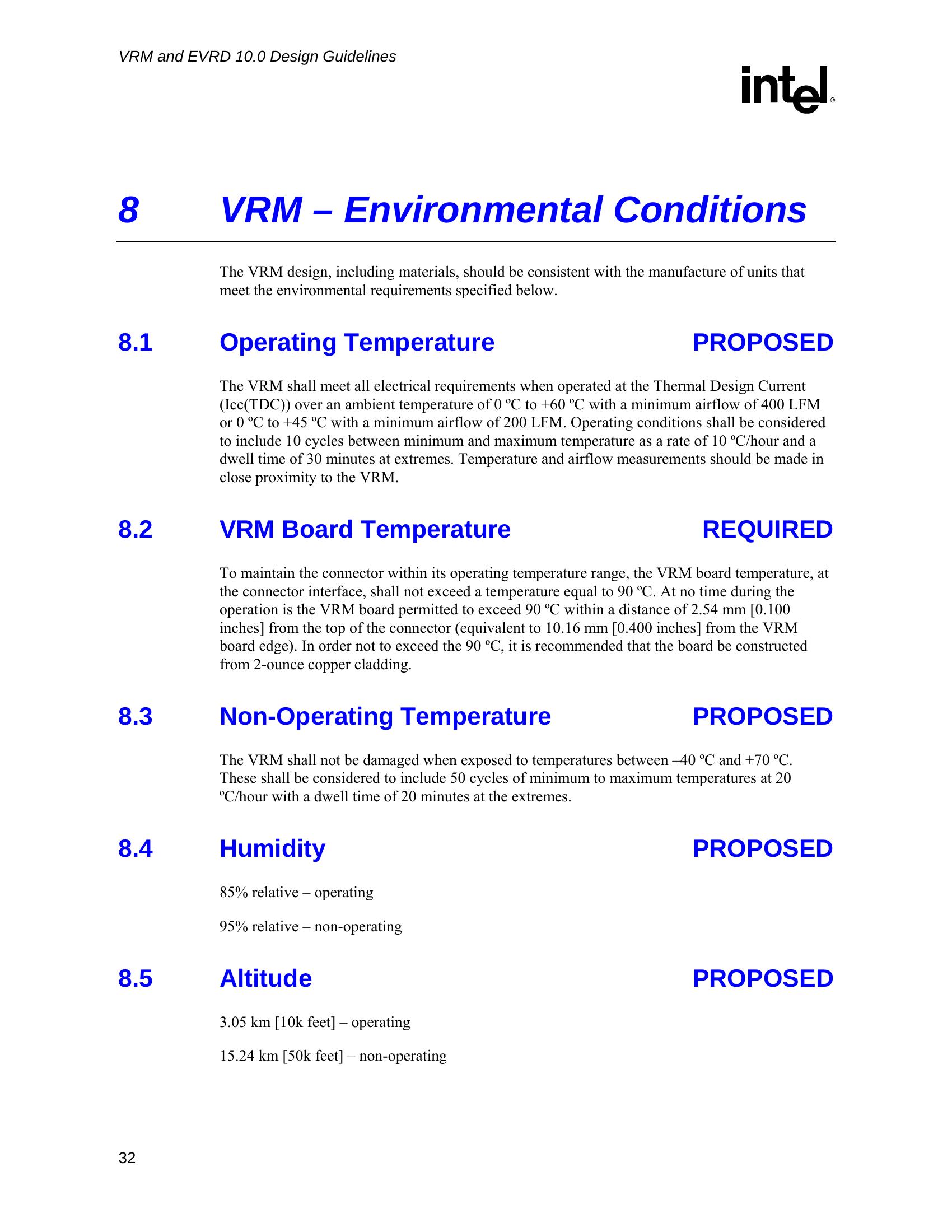
8 VRM – Environmental Conditions
The VRM design, including materials, should be consistent with the manufacture of units that
meet the environmental requirements specified below.
8.1 Operating Temperature PROPOSED
The VRM shall meet all electrical requirements when operated at the Thermal Design Current
(Icc(TDC)) over an ambient temperature of 0 ºC to +60 ºC with a minimum airflow of 400 LFM
or 0 ºC to +45 ºC with a minimum airflow of 200 LFM. Operating conditions shall be considered
to include 10 cycles between minimum and maximum temperature as a rate of 10 ºC/hour and a
dwell time of 30 minutes at extremes. Temperature and airflow measurements should be made in
close proximity to the VRM.
8.2 VRM Board Temperature REQUIRED
To maintain the connector within its operating temperature range, the VRM board temperature, at
the connector interface, shall not exceed a temperature equal to 90 ºC. At no time during the
operation is the VRM board permitted to exceed 90 ºC within a distance of 2.54 mm [0.100
inches] from the top of the connector (equivalent to 10.16 mm [0.400 inches] from the VRM
board edge). In order not to exceed the 90 ºC, it is recommended that the board be constructed
from 2-ounce copper cladding.
8.3 Non-Operating Temperature PROPOSED
The VRM shall not be damaged when exposed to temperatures between –40 ºC and +70 ºC.
These shall be considered to include 50 cycles of minimum to maximum temperatures at 20
ºC/hour with a dwell time of 20 minutes at the extremes.
8.4 Humidity PROPOSED
85% relative – operating
95% relative – non-operating
8.5 Altitude PROPOSED
3.05 km [10k feet] – operating
15.24 km [50k feet] – non-operating
32
| None | |
| None | |
VRM and EVRD 10.0 Design Guidelines
R
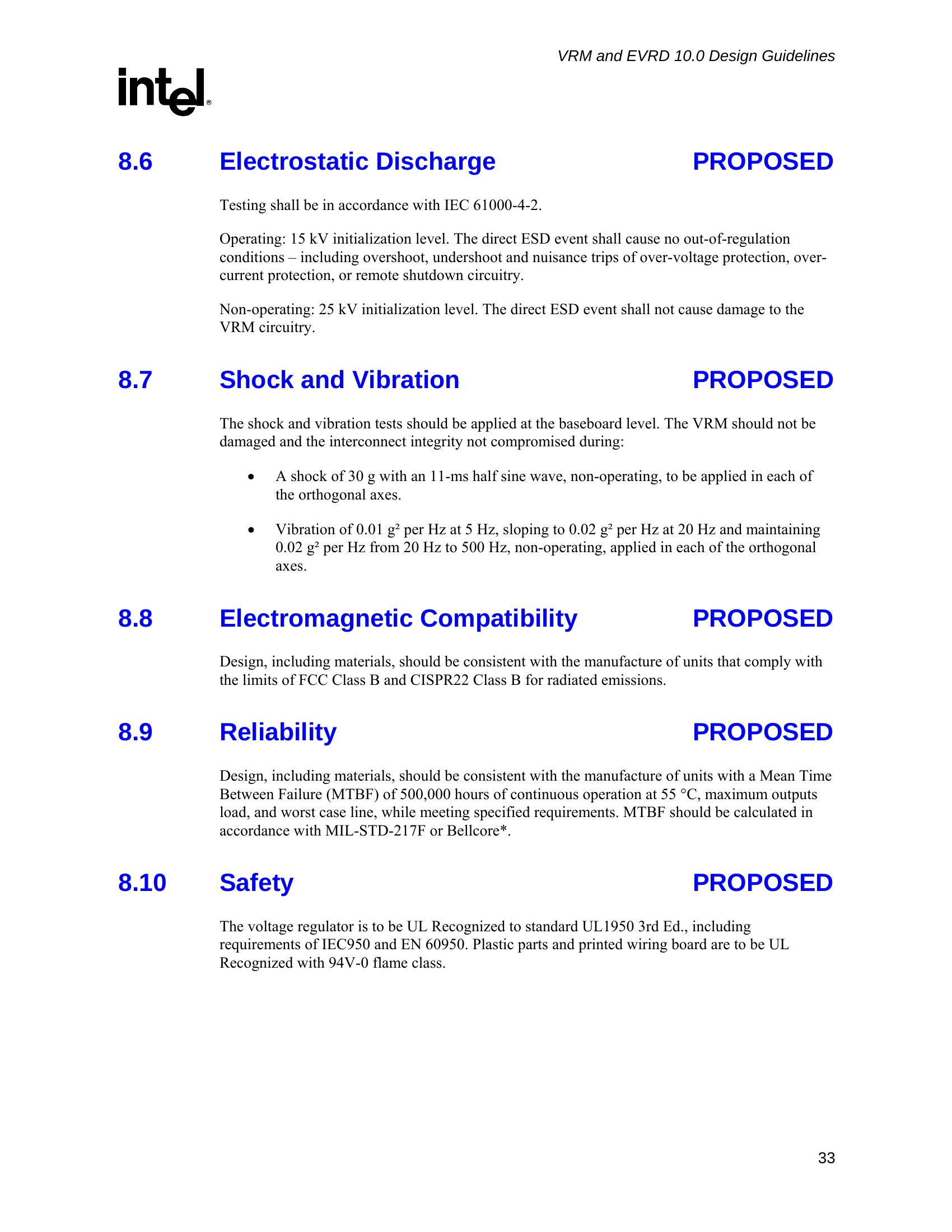
8.6 Electrostatic Discharge PROPOSED
Testing shall be in accordance with IEC 61000-4-2.
Operating: 15 kV initialization level. The direct ESD event shall cause no out-of-regulation
conditions – including overshoot, undershoot and nuisance trips of over-voltage protection, over-
current protection, or remote shutdown circuitry.
Non-operating: 25 kV initialization level. The direct ESD event shall not cause damage to the
VRM circuitry.
8.7 Shock and Vibration PROPOSED
The shock and vibration tests should be applied at the baseboard level. The VRM should not be
damaged and the interconnect integrity not compromised during:
• A shock of 30 g with an 11-ms half sine wave, non-operating, to be applied in each of
the orthogonal axes.
• Vibration of 0.01 g² per Hz at 5 Hz, sloping to 0.02 g² per Hz at 20 Hz and maintaining
0.02 g² per Hz from 20 Hz to 500 Hz, non-operating, applied in each of the orthogonal
axes.
8.8 Electromagnetic Compatibility PROPOSED
Design, including materials, should be consistent with the manufacture of units that comply with
the limits of FCC Class B and CISPR22 Class B for radiated emissions.
8.9 Reliability PROPOSED
Design, including materials, should be consistent with the manufacture of units with a Mean Time
Between Failure (MTBF) of 500,000 hours of continuous operation at 55 °C, maximum outputs
load, and worst case line, while meeting specified requirements. MTBF should be calculated in
accordance with MIL-STD-217F or Bellcore*.
8.10 Safety PROPOSED
The voltage regulator is to be UL Recognized to standard UL1950 3rd Ed., including
requirements of IEC950 and EN 60950. Plastic parts and printed wiring board are to be UL
Recognized with 94V-0 flame class.
33
| None | |
| None | |
VRM and EVRD 10.0 Design Guidelines
R
9 Manufacturing Considerations
9.1 Lead Free (Pb Free)
Intel recommends that designers be aware of legislation regarding the use of lead in computer
products such as the European Union (EU) Restriction on Hazardous Materials directive, also
known as RoHS (commonly pronounced ‘rowhass’). The commission directive may be found at
the following URL:
http://europa.eu.int/eur-lex/pri/en/oj/dat/2003/l_037/l_03720030213en00190023.pdf
For the latest information on RoHS please refer to the following URL:
http://europa.eu.int/eur-lex/en
Intel recommends that you consider Pb Free manufacturing processes and components for the
module and connector.
34
| None | |
| None | |
VRM and EVRD 10.0 Design Guidelines
R
35
| None | |
| None | |


