VRM circuit building blocks:
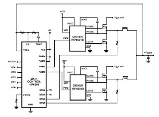
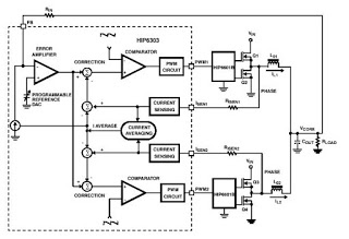
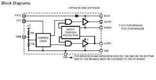
VRM module circuit usually by HIP630X series and HIP660X series chips, which were the chips and a variety of different models, with some differences. Icon for the HIP6301 and HIP6601 VRM modules comprising circuit.
VRM modules describe the overall function of the circuit: HIP6301 chip’s role is to get two-phase complementary PWM signal to the power supply for GPU Switching to provide the required voltage; Each output of the PWM signal and are connected with a HIP6601 chip. PWM signal is a periodic square wave signal is high when the PWM1, PWM2 is low, UGATE1 open, high, so that its pipe connecting the MOS Q1 is turned on, and LGATE1 low, Q2 off; At the same time, because PWM2 is low, UGATE2 off, LGATE2 open, so turn off Q3, Q4 turned on, so this time the input voltage Vin will be through Q1 and Q4, and obtained by the superposition of the GPU voltage required core voltage Vcore; the next moment, PWM1 to go low, PWM2 goes high, Q2, Q3 turns on, Q1 and Q4 turn off, so this is a moment of Vcore Vin Diego through Q2 and Q3 obtained after the increase.
Next we will study and analyze HIP6601 and HIP6301 chips.
HIP6301 Functional Analysis
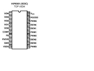
HIP6301 external package icon below
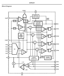
HIP6301 internal circuit illustrated below
Pin Description:
VID4 (Pin 1), VID3 (Pin 2), VID2 (Pin 3), VID1 (Pin 4) 和 VID0 (Pin 5):
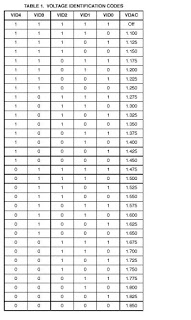
3.3 V logic level, the equivalent voltage identification of the role of different groups and the logic level voltage output corresponding to different values, HIP6301 through these five levels of decoding the corresponding Vcore value, corresponding to the parameters of the table below, When five high average power value, the circuit closed.
HIP6301 internal circuit)
Pin Description:
VID4 (Pin 1), VID3 (Pin 2), VID2 (Pin 3), VID1 (Pin 4) 和 VID0 (Pin 5):
3.3 V logic level, the equivalent voltage identification of the role of different groups and the logic level voltage output corresponding to different values, HIP6301 through these five levels of decoding the corresponding Vcore value, corresponding to the parameters of the table below, When five high average power value, the circuit closed.
Pin Description:
VID4 (Pin 1), VID3 (Pin 2), VID2 (Pin 3), VID1 (Pin 4) 和 VID0 (Pin 5):
3.3 V logic level, the equivalent voltage identification
of the role of different groups and the logic level voltage output corresponding to different values, HIP6301 through these five levels of decoding the corresponding Vcore value, corresponding to the parameters of the table below, When five high average power value, the circuit closed.
COMP (Pin 6):
And the internal circuitry of the error amplifier (E A) connected to the output, with the sawtooth generator (SAWTOOTH GENERATOR) comparisons of PWM voltage signal;
FB (Pin 7) :
Feedback signal, is connected with the output of Vcore;
FS / DIS (Pin 8):
With a resistor connected to ground Rt, Rt behind the decision of the size of the conversion clock frequency HIP6301 size, if the pin directly to ground, leading to the back of the converter circuit is closed;
GND (Pin 9): 接地
VSEN (Pin 10):
Power good电压的输入,与Vcore相连;
PWM1 (Pin 15), PWM2 (Pin 14), PWM3 (Pin 11) 和 PWM4 (Pin 18):
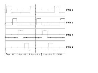
Pulse-Width Modulation, pulse width modulation signal is alternating phase rectangular wave signals to each other, driving up and down the back of the HIP6301 to control rotation of the two MOS conduction. When only three groups when the PWM signal should be tied high PWM4; when only two groups when the PWM signal should be tied high while PWM3 and PWM4. Here are four of the PWM signal wave
ISEN1 (Pin 16), ISEN2 (Pin 13), ISEN3 (Pin 12) 和 ISEN4 (Pin 17):
Current pin, connected to the PHASE node, the current input to the GPU diversion effect when certain pins when not in use, it should be suspended;
PGOOD (Pin 19):
Connected to the Vcore voltage of the Vcore from the surveillance role, when its value within the specified range, the voltage is high;
VCC(Pin 20) :
Connected to 5V operating voltage.
Analysis of the specific module circuit
PWM signal generation, current, voltage compensation circuit module
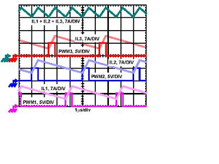
First, the analysis of the current, set into the side of the current signal to the Vcore is Iout, then each channel will Iout PHASE symmetrical current shunt, the relevant waveform as shown (3 PHASE channel)
Iout current frequency of visible size of each channel will be the size of three times the current frequency (3 PHASE channel), and since each channel current intertwined, making the final changes in current amplitude after superposition (ie, the magnitude of Iout) be reduced, so that an external capacitor to reduce power consumption.
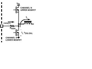
Each channel shunt current will be obtained through the IL into the Isen pin the PHASE node, the corresponding curre
In and IL of the relationship:
Rds (on) is located below the LOWER MOSFET inductance of D, S pole on-resistance values between
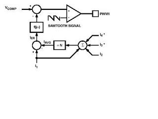
In the current of each pin will be added through the addition CURRENT AVERAGE N module circuit obtained after an average current value Iavg, the relevant circuit (4 PHASE-channel) as follows
(4 PHASE通道)
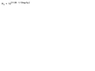
In the current of each pin and then will be compared with the current Iavg get Ier difference current. As the current phase of each channel of IL staggered, so streaming down In the current phase is still interlaced, and in comparison with Iavg amplitude by a frequency converter f (jw), the phase value obtained just intertwined, so Vcomp signal compared with the sawtooth signal voltage obtained by phase PWM signal will also be intertwined rectangular wave signal. PWM waveform frequency Fs and HIP6301 pin FS / DIS (Pin 8) are then related to the size of the Rt, the specific relationship is as follows
When the Vcore end of the current, voltage fluctuations generated within the provisions, HIP6301 chip with automatic current, voltage compensation, in order to determine the output side of the current lead Vcore voltage to maintain a stable work values.
Current compensation analysis (Current Loop): Each PWM channel has its own independent current value, it will be with the CURRENT AVERAGE module circuit current of Iavg compare PWM channel at a time if too much current, then, by comparing the module to be The difference in current will increase Ier (note the amplitude of the frequency converter), which would cause the input to the voltage comparator (COMPARATOR) is an extreme level of voltage increase, so that the voltage comparator output signal PWM square wave of width reduction small, and thus regain control of the HIP6301 chip output current to return to a stable value.
Voltage compensation analysis (Voltage Loop): basic principles with the same current compensation function, but its end is the feedback control signal pin FB (Pin 7) phase of the internal error amplifier (ERROR AMPLIFIER). Because FB is connected with the Vcore voltage, CPU core voltage so as to reduce at a time when, with the positive terminal of the voltage error amplifier signal VDAC (ie 5-digit level by the VID DAC reference voltage obtained by value) will increase large, thereby connecting the voltage amplifier with PWM control signal changes, in order to achieve re-stabilize the purpose of the GPU core voltage.
Compensation and current compensation voltage difference:
1.
2.
Soft – Star modules, circuit protection module error analysi
When the V cc voltage reaches 4.375V after, PWM signal will be transferred to the work of state and Soft-Star module circuit will officially work. If the voltage V cc at a time down to 3.875V in the following words, POR module will once again shut down converter circuit, the output of the PWM signal at the third state, MOS tube closure.
Soft – Star module circuit analysis: once when the V cc voltage reaches 4.375V after, PWM signal will be transferred to the working state, then Soft-Star module circuit will also be a formal job, 5 VID logic level through DAC get VDAC voltage, VDAC voltage increases from zero size is a process, Soft-Star module circuit by controlling the error amplifier will also be E A so that the final output of the GPU core voltage Vcore is a slow increase of the process and stabilized at the size of the final regulations. During this process there is a delay, let’s specific analysis.
Because the PWM signal has become active, in its first 32 clock cycles of time, DAC modul
e output will be in a state of suppression, the output of the PWM signal will be in a third state; from the first clock cycle will be 33 a short time interval, PWM output voltage remains low, here the error amplifier E A, sawtooth generator, voltage comparator, and other functional circuit blocks will begin to enter the normal working condition; during this interval, the output bandwidth of the PWM pulse signal will gradually increase, thus driving the back of MOS, the output voltage to the GPU side gradually increased, and in 2048 clock cycles before reaching the core voltage. Therefore, the length of the delay time DT = 2048 Fsw, in 2048 clock cycles, PGOOD formally initialized.
For example, if Fsw to 200KHZ, then the first 32 clock cycles, that is 160US time the PWM output signal is the third state, after which period of time between arrival and until 2048, when the clock cycle, PWM pulse signal bandwidth will gradually increase the output voltage will gradually increase to the value of work during the delay time for 10.08MS, so the total size of the delay time:
DT = 2048 200k = 10.24ms
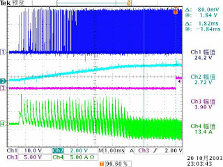
Related waveform as shown:
CH1:PWM CH2: Vcore CH3: PGOOD
Voltage protection module error: When the voltage exceeds the output voltage of 15% or below the set output voltage of 10% will trigger the two UV and OVP protection circuit module, the PGOOD output voltage goes low, thereby the output of the PWM signal is the third state, MOS tube closure;
Current fault protection module: basically the same principles with the voltage protection, output current with a reference current I-trip comparison, when the output current is too high, OC modules will be driven by Soft-Star module circuit delay time increased, so that the output The PWM signal is the third state or low, MOS tube closure;
HIP6601 Functional Analysis
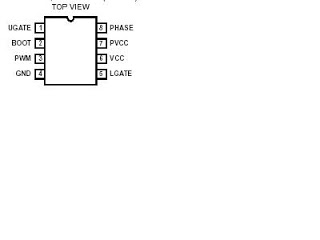
Chip package icon:
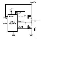
And outside of the original of 连接:
Pin Description:
UGATE(Pin 1): Upper gate驱动,与外部的high-side MOS相连,驱动其开启或关闭;
BOOT(Pin 2): 通过一电容(bootstrap capacitor)与PHASE脚相连,bootstrap capacitor的作用是控制high-side MOS的开启;
PWM (Pin 3): the chip input drive signal from the front of the HIP6301 chip production;
GND (Pin 4): 接地 引脚;
LGATE(Pin 5): Lower gate驱动,与外部的low-side MOS相连,驱动其开启或关闭;
VCC (Pin 6): chip voltage, then the 12V level;
PVCC (Pin 7): Upper gate drive voltage, typically in the range between 5V —– 12V;
PHASE (Pin 8): connections between the two MOS tube, the voltage by an internal breakdown protection circuit module to be monitored, but also the role of feedback;
HIP6601 internal circuit illustrated belowHIP6601 internal circuit)
Analysis module:
Chip operating voltage VCC reaches the rated value before, Ugate and Lgate remain closed. Once VCC reaches the working value, PWM signal will begin to control two doors up and down
When the PWM signal into the HIP6601, the first open door is LGATE, because when the PWM signal is controlled by CONTROL LOGIC circuit, divided into “1” and “2” two-way digital signal, and the two signals differ, that is (1,0) or (0,1), but taking into account the specific circuit, only (0,1), anti-column proof: If (1,0), then UGATE turn, LGATE close, high-side MOS open, and the formation of channel voltage above 12V, this time not because Bootstrap Capacitor charging process, so Vboot = Vbc +12 V = 12V, so UGATE previously connected the control module can not be opened, the signal will not output to UGATE up.
击穿保护功能分析(Shoot—-Through Protection):
In fact, through two digital level “3”, “4” to control UGATE and LGATE opening, to prevent two doors open simultaneously to cause the circuit breakdown. Shoot —- Through Protection of the feedback signal input termination PHASE, by monitoring the voltage output signal to control the size of “3” “4” level of high and low. During the closed door in UGATE, Shoot —- Through Protection will monitor the voltage of PHASE, PHASE once the voltage drops to 0.5V, the output control signal “3” “4” will drive LGATE gate ready to open if the voltage PHASE in 250ns time can not be reduced to below 0.5V, and continue to maintain a high potential of more than 2us time, then the output of the “3” “4” will LGATE off, while maintaining that UGATE and LGATE low until the next PWM pulse Driver HIP6601 work again before the signal.


